An identification chip and its manufacturing method

A production method and chip technology, which is applied in the field of identification chips, can solve the problems of difficult identification of different chip chip electrodes, achieve the effects of reducing scrap rate and production cost, increasing brand recognition, improving chip identification rate and production efficiency

Inactive Publication Date: 2019-02-01
山东影响力智能科技有限公司
View PDF6 Cites 0 Cited by
  • Summary
  • Abstract
  • Description
  • Claims
  • Application Information

AI Technical Summary

Problems solved by technology

[0005] In view of the shortcomings of the prior art described above, the purpose of the present invention is to provide an identification chip and its manufacturing method, which is used to solve the problem that different chips or chip electrodes are difficult to identify in the prior art

Method used


Image

  • An identification chip and its manufacturing method
  • An identification chip and its manufacturing method
  • An identification chip and its manufacturing method

Examples


Embodiment 1

[0035] Such as Figure 1-13 Shown, the present invention provides a kind of manufacturing method of LED identification chip, and manufacturing method comprises the following steps at least:

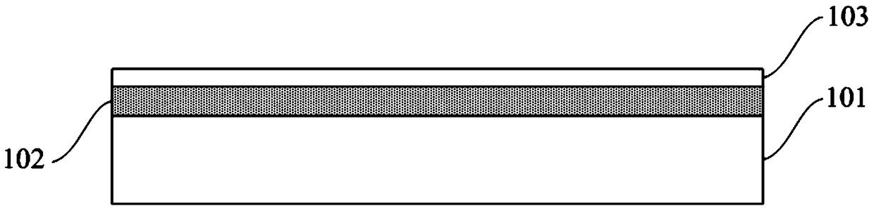
[0036] Such as figure 1 As shown, step S1 is first performed to provide a growth substrate 101 and form a light-emitting epitaxial layer 102 on the upper surface of the growth substrate 101 . In this embodiment, the growth substrate 101 can be sapphire (Al 2 o 3 ), the light-emitting epitaxial layer 102 includes an N-GaN light-emitting epitaxial layer. Then step S2 is executed.

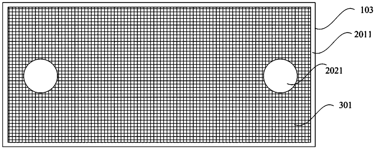
[0037] Such as figure 1 with figure 2 As shown, in step S2 , a transparent conductive layer 103 is formed on the upper surface of the light emitting epitaxial layer 102 . First, if figure 1 As shown, a transparent conductive layer 103 is formed on the surface of the light-emitting epitaxial layer 102 by evaporation or sputtering. Then, a photoresist layer 301 is formed on the transparent conductive la...

Embodiment 2

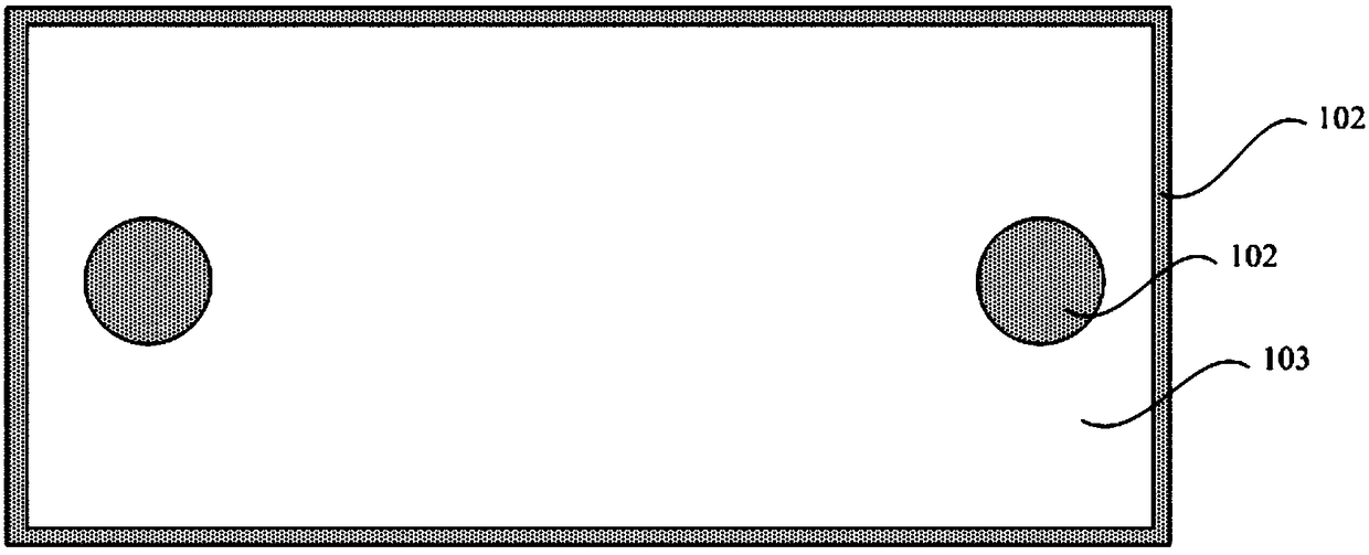
[0047] The present invention also provides an identification chip, such as Figure 14 As shown, the identification chip 1 includes: a growth substrate 101 , a light-emitting epitaxial layer 102 , a transparent conductive layer 103 , a mirror layer 104 , a barrier layer 105 , an N electrode diffusion layer 106 , a passivation layer 107 , and an electrode 108 .

[0048] For better understanding, please refer to Figure 1 to Figure 14 , as shown in the figure, the identification chip contains:

[0049] Growth substrate 101, in the present embodiment, growth substrate 101 can be sapphire (Al 2 o 3 ), silicon (Si) or silicon carbide (SiC).

[0050] The light emitting epitaxial layer 102 is formed on the upper surface of the growth substrate 101 . In this embodiment, the light emitting epitaxial layer 102 includes an N-GaN light emitting epitaxial layer. The light-emitting epitaxial layer 102 has a first scribe region 2011 and a first N hole region 2021 , at least one of the fi...


PUM


Abstract

The invention provides an identification chip and a manufacturing method thereof. The manufacturing method of the identification chip comprises the following steps that 1) an epitaxial structure is provided, a barrier layer is formed on the epitaxial structure, and the barrier layer is etched or corroded so as to form an N-hole region and a P-hole region; 2) an N-electrode diffusion layer is manufactured and used for electrical lead-out of the N-hole region; and 3) a passivation layer is grown, and the passivation layer is etched or corroded to form a first reserved region and a second reserved region, wherein the first reserved region is corresponding to the P-hole region, and the first reserved region and the second reserved region include the specific identification information. The identification chip comprises a growing substrate, a lighting epitaxial layer, a transparent conductive layer, a reflecting mirror layer, the barrier layer, the N-electrode diffusion layer, the passivation layer and electrodes which are arranged from the bottom to the top in turn. The identification chip and the manufacturing method thereof can be used for solving the problems in the prior art that different chips of chip electrodes are difficult to identify.

Description

technical field [0001] The invention relates to an identification chip, in particular to an identification chip and a manufacturing method thereof. Background technique [0002] The automatic machines used in the production and testing process of light-emitting diodes (Light Emitting Diode, referred to as LED), specifically including Die Bonder, Wire Bonder and Chip Prober, etc. Pattern Recognition (Pattern Recognition) function to determine the correct position of the chip and guide the movement of the machine. [0003] Metal electrodes are the most obvious structure on the LED chip and are easy to interpret. Therefore, the pattern of metal electrodes has always been used as the basis for image recognition. The adoption of new technologies to improve chip brightness, such as Surface Roughen and Patterned Sapphire Substrate, often causes changes in the gray scale of the CCD image, making it difficult to distinguish metal electrodes. Moreover, the typical size of the LED ch...

Claims


Application Information

Patent Timeline
Patent Type & Authority Patents(China)
IPC IPC(8): H01L33/00H01L33/48
CPCH01L33/005H01L33/48H01L2933/0008
Inventor 杨杰常文斌林宇杰
Owner 山东影响力智能科技有限公司
Why Eureka
Try Eureka