Film tearing station for thinned silicon wafer processing

A technology for consoles and silicon wafers, applied to semiconductor devices, electrical components, circuits, etc., can solve the problems of uneven force on silicon wafers, affecting device performance, easy to scratch silicon wafers, etc., to achieve uniform force and convenient operation Good sex, good protective effect

Active Publication Date: 2019-07-12
THE 44TH INST OF CHINA ELECTRONICS TECH GROUP CORP
View PDF2 Cites 0 Cited by
  • Summary
  • Abstract
  • Description
  • Claims
  • Application Information

AI Technical Summary

Problems solved by technology

[0002] When thinning the silicon wafer, it is necessary to frequently transfer the silicon wafer to different operating platforms to complete various processing techniques; since the photosensitive structure has been pre-fabricated on the front of the silicon wafer, in order to avoid If the photosensitive structure is scratched, a protective film is usually mounted on the front of the silicon wafer, and the protective film is torn off after the thinning process is completed. Since the structural strength of the thinned silicon wafer (especially the ultra-thin silicon wafer) is very fragile, Therefore, the degree of refinement of the film tearing operation is high, and it is usually carried out manually. In the specific operation, the silicon wafer is generally placed on a solid table with the back side down for the film tearing operation. The existing problem is: in the process of thinning , the back of the silicon wafer has been polished with high precision. If the polished surface is damaged, it will affect the performance of the device; when the film is torn off, the contact area between the polished surface of the silicon wafer and the solid table is large, and the solid table is easy to exist. Tiny particles. In order to separate the protective film from the silicon wafer, the operator needs to apply force to the edge of the protective film and the silicon wafer at the same time. During the force application process, the tiny particles on the solid table are likely to scratch the silicon wafer. In severe cases, the tiny particles will cause Uneven stress on silicon wafers and fragments

Method used


Image

  • Film tearing station for thinned silicon wafer processing
  • Film tearing station for thinned silicon wafer processing
  • Film tearing station for thinned silicon wafer processing

Examples


Embodiment Construction

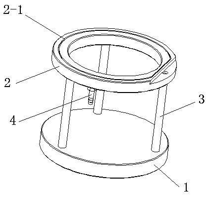
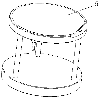
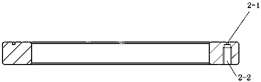
[0011] A film tearing console for thinning silicon wafer processing, the innovation of which is that the tearing film console is composed of a base 1, a support plate 2, a plurality of connecting columns 3 and a connection nozzle 4; the support plate 2 is An annular structure, the upper end surface of the support plate 2 forms an operating surface, the operating surface is provided with an annular groove, the annular groove is located at the periphery of the inner hole of the support plate 2, and a connecting hole is arranged on the lower end surface of the support plate 2, connecting The bottom of the hole communicates with the bottom of the annular groove, and the upper end of the connection nozzle 4 is sleeved in the connection hole; the support plate 2 is arranged directly above the base 1, and the upper end surface of the support plate 2 and the lower end surface of the base 1 Parallel; the upper end of the connecting column 3 is connected with the lower end surface of the...


PUM


Abstract

The invention discloses a film-tearing operation platform for thinned silicon wafer processing. The film-tearing operation platform comprises a pedestal, a supporting plate, multiple connecting columns and a connecting nozzle. The beneficial technical effects of the invention are as follows: according to the film-tearing operation platform for the thinned silicon wafer processing, the film-tearing operation platform can take relatively good protective effect to a middle part of a silicon wafer, so that the occurrence of a fragmentation condition is effectively avoided; and the operation convenience is relatively good.

Description

technical field [0001] The invention relates to an ultra-thin silicon chip processing technology, in particular to a film-tearing operation table for thin silicon chip processing. Background technique [0002] When thinning the silicon wafer, it is necessary to frequently transfer the silicon wafer to different operating platforms to complete various processing techniques; since the photosensitive structure has been pre-fabricated on the front of the silicon wafer, in order to avoid If the photosensitive structure is scratched, a protective film is usually mounted on the front of the silicon wafer, and the protective film is torn off after the thinning process is completed. Since the structural strength of the thinned silicon wafer (especially the ultra-thin silicon wafer) is very fragile, Therefore, the degree of refinement of the film tearing operation is high, and it is usually carried out manually. In the specific operation, the silicon wafer is generally placed on a sol...

Claims


Application Information

Patent Timeline
Patent Type & Authority Patents(China)
IPC IPC(8): H01L21/683
CPCH01L21/6835H01L2221/68386
Inventor 江海波胡莉娟陶启林邓刚王晓强
Owner THE 44TH INST OF CHINA ELECTRONICS TECH GROUP CORP
Why Eureka
Try Eureka