Flexible substrate and manufacturing method thereof

A flexible substrate and manufacturing method technology, applied in the direction of climate sustainability, final product manufacturing, sustainable manufacturing/processing, etc., can solve the problem of reducing the light reflectivity of the alignment mark, affecting the alignment success rate, reducing the coverage area, etc. problem, achieve the effect of avoiding etching residue, high alignment success rate, and reducing coverage area

Inactive Publication Date: 2017-04-26
WUHAN CHINA STAR OPTOELECTRONICS TECH CO LTD
View PDF4 Cites 3 Cited by
  • Summary
  • Abstract
  • Description
  • Claims
  • Application Information

AI Technical Summary

Problems solved by technology

However, the larger the coverage area of ​​the organic material substrate on the carrier glass substrate, the greater the warpage of the organic material substrate during the array process, and the lower the production yield. Therefore, we need to ensure the production of various alignment marks. Minimize its footprint on the carrier glass substrate while on the organic material substrate
[0005] Based on the layout design and equipment specifications in actual production, take the OLED evaporation alignment Mark in the series Mark closest to the edge of the substrate as an example. Due to the large viscosity coefficient of the organic material used in the flexible organic material substrate, the flexible organic material The edge of the material substrate will form a very steep angle, which will easily cause etching residues and other phenomena at this position, and since the flexible organic material substrate in OLED flexible display devices made of LTPS materials is mostly made of colored and high-temperature resistant organic materials, the evaporation alignment When the alignment light source enters from the back of the flexible organic material substrate and passes through the colored flexible organic material substrate, it will cause light loss, reduce the light reflectivity of the alignment mark, and affect the success rate of alignment

Method used


Image

  • Flexible substrate and manufacturing method thereof
  • Flexible substrate and manufacturing method thereof
  • Flexible substrate and manufacturing method thereof

Examples


Embodiment Construction

[0029] In order to further illustrate the technical means adopted by the present invention and its effects, the following describes in detail in conjunction with preferred embodiments of the present invention and accompanying drawings.

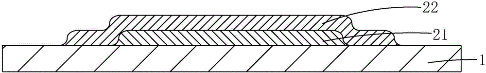
[0030] Please also see figure 1 and figure 2 , the present invention firstly provides a flexible substrate, including a first organic material layer 21 laid on the carrier substrate 1 , and a second organic material layer 22 completely covering the first organic material layer 21 . The coverage area of ​​the second organic material layer 22 on the carrier substrate 1 is larger than the coverage area of ​​the first organic material layer 21 on the carrier substrate 1, and the long side edge of the second organic material layer 22 surrounds the long side of the first organic material layer 21 edge.

[0031] Specifically, the carrier substrate 1 is preferably a glass substrate; the material of the first organic material layer 21 and the second...


PUM


Abstract

The invention provides a flexible substrate and a manufacturing method thereof. The flexible substrate is divided into a first organic material layer (21) and a second organic material layer (22), the coverage area of the second organic material layer (22) on a carrier substrate (1) is larger than the coverage area of the first organic material layer (21) on the carrier substrate (1), the long edge of the second organic material layer (22) surrounds the long edge of the first organic material layer (21), so that the thickness of the edge of the flexible substrate is reduced, the etching residue at the edge can be avoided, the coverage area of the organic material on the carrier substrate is reduced, and the warpage of the flexible substrate is reduced. In addition, an aligning mark (3) is arranged on the second organic material layer (22) between the long edge of the second organic material layer (22) and the long edge of the first organic material layer (21), so that the aligning precision of the subsequent vapor plating processes can be guaranteed, and because only one layer of organic material is arranged at the aligning mark (3), the light transmittance is increased and the aligning success rate is improved.

Description

technical field [0001] The invention relates to the field of display technology, in particular to a flexible substrate and a manufacturing method thereof. Background technique [0002] Organic Light Emitting Display (OLED) OLED is a display technology with great development prospects. It not only has excellent display performance, but also has self-illumination, simple structure, ultra-thin, fast response, wide Viewing angle, low power consumption and flexible display are known as "dream display", which has been favored by major display manufacturers and has become the main force of the third-generation display devices in the field of display technology. [0003] A flexible OLED display device requires an array of pixel structures distributed on a substrate, and each pixel structure generally includes thin film transistors (Thin Film Transistor, TFT), capacitors and other components. [0004] At present, OLED flexible display devices are generally prepared on the basis of o...

Claims


Application Information

Patent Timeline
Patent Type & Authority Applications(China)
IPC IPC(8): H01L27/32H01L51/00H01L51/56H01L51/50
CPCH10K59/12H10K77/111H10K71/00Y02E10/549Y02P70/50
Inventor 秦芳
Owner WUHAN CHINA STAR OPTOELECTRONICS TECH CO LTD
Why Eureka
Try Eureka