Hole plugging method of PCB

A technology of plug holes and front holes, which is applied in the direction of electrical connection formation of printed components, electrical components, printed circuits, etc., can solve the problems of difficulty in making outer layer circuits, reduce the uniformity of outer layer copper layer thickness, and high product defect rate, and achieve The effect of improving production capacity, reducing the number of grinding plates, and improving production efficiency

Inactive Publication Date: 2017-04-05
SHENZHEN SUNTAK MULTILAYER PCB
View PDF4 Cites 8 Cited by
  • Summary
  • Abstract
  • Description
  • Claims
  • Application Information

AI Technical Summary

Problems solved by technology

[0003] The present invention aims at the existing resin / copper paste hole plugging technology. Before filling the hole with resin / copper paste, the electroplating hole process needs to be carried out, and the multi-layer production board needs to be ground in the electroplating hole process, and the number of grinding plates increases. It will reduce the uniformity of the thickness of the outer copper layer of the multi-layer production board, resulting in difficulties in making the outer layer circuit and high product defect rate. A method of plugging holes without the need for electroplating holes is provided.

Method used


Image

  • Hole plugging method of PCB
  • Hole plugging method of PCB

Examples


Embodiment 1

[0017] This embodiment provides a method for manufacturing a PCB, in which copper paste plug holes need to be manufactured on the PCB. And in order to illustrate the technical content of the present invention, the holes on the PCB of this embodiment are designed to be plugged with copper paste, and there is no need to make other metallized holes and metallized holes filled with other materials.

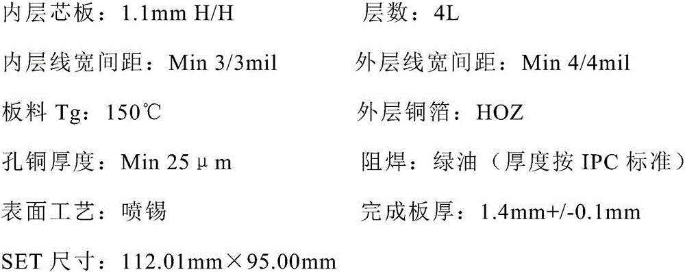
[0018] The specification parameters of the prepared PCB are as follows:

[0019]

[0020] Specific steps are as follows:

[0021] (1) Multi-layer production board

[0022] According to the existing technology, the inner layer core board and the outer layer copper foil are made into a multi-layer production board through the process of material cutting → negative film making of the inner layer circuit → pressing → drilling → copper sinking → full board electroplating, that is, the inner layer core board and the outer layer copper foil are made into a multi-layer production board T...

Embodiment 2

[0054] This embodiment provides a method for manufacturing a PCB, in which copper paste plug holes need to be manufactured on the PCB. In addition to the copper paste plug holes, other metallized holes (such as metallized through holes and metallized blind holes) need to be formed on the PCB of this embodiment.

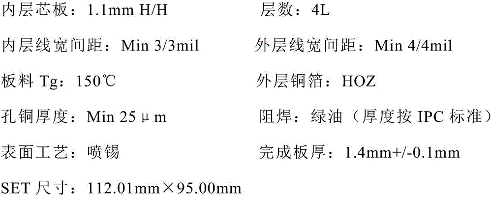
[0055] The specification parameters of the prepared PCB are as follows:

[0056]

[0057] Specific steps are as follows:

[0058] (1) Multi-layer production board

[0059] According to the existing technology, the inner layer core board and the outer layer copper foil are made into a multi-layer production board through the process of material cutting → negative film making of the inner layer circuit → pressing → drilling → copper sinking → full board electroplating, that is, the inner layer core board and the outer layer copper foil are made into a multi-layer production board The core board, the prepreg and the outer copper foil are laminated into one productio...


PUM


Abstract

The invention relates to the technical field of production of circuit boards, and specifically relates to a hole plugging method of a PCB. According to the method, copper paste is directly plugged into pre-plugging holes on a multi-layer production plate, the process of hole electroplating in the conventional copper paste hole-plugging technology is omitted, the frequency of plate polishing in a production process is reduced, the non-uniformity degree of the thickness of an external copper layer of the multi-layer production plate is reduced, the uniformity of an external line is guaranteed, guarantee is provided for the manufacture of the external line, and the manufacturing capability of the external fine line is improved. Besides, according to the method, the process of hole electroplating is avoided, multiple steps of film pasting, exposure, development and electroplating etc. in the process of hole electroplating are correspondingly reduced, the technical process is optimized, and the production efficiency is improved.

Description

technical field [0001] The invention relates to the technical field of circuit board production, in particular to a method for plugging holes in a PCB. Background technique [0002] PCB (Printed Circuit Board), the Chinese name is printed circuit board, also known as printed circuit board. The production of PCB includes two links of circuit design and manufacturing. The manufacture of PCB is based on the previous circuit design. The manufacturing process is generally as follows: according to the design requirements, the inner core board is cut into the required size in the cutting process→inside Lay film on the core board → use the inner layer film to expose in position → develop and remove the uncured film to form an inner layer pattern → etch the copper layer not covered by the film on the inner core board to form an inner layer circuit → fade the film → put The inner core boards are stacked in a certain order and combined by high temperature pressure to form a multi-laye...

Claims


Application Information

Patent Timeline
Patent Type & Authority Applications(China)
IPC IPC(8): H05K3/42
CPCH05K3/42H05K2201/09563
Inventor 周文涛姜雪飞宋清翟青霞
Owner SHENZHEN SUNTAK MULTILAYER PCB
Why Eureka
Try Eureka