Method and system for extracting semiconductor defect level

A defect energy level, semiconductor technology, applied in the direction of single semiconductor device testing, instruments, measuring devices, etc., can solve the problem of inability to extract the defect energy level and defect surface density of the gate dielectric layer in nMOS devices, so as to improve device performance and The effect of reliability

Inactive Publication Date: 2017-04-05
INST OF MICROELECTRONICS CHINESE ACAD OF SCI
View PDF2 Cites 6 Cited by
  • Summary
  • Abstract
  • Description
  • Claims
  • Application Information

AI Technical Summary

Problems solved by technology

[0005] The present invention aims to solve the problem that the prior art cannot extract the defect energy level, defect surface density, and the relationship between the defect energy level and the defect surface density of the gate dielectric layer in nMOS devices, and provides a method for extracting semiconductor defect energy levels and systems to improve device performance and reliability

Method used


Image

  • Method and system for extracting semiconductor defect level
  • Method and system for extracting semiconductor defect level
  • Method and system for extracting semiconductor defect level

Examples


Embodiment Construction

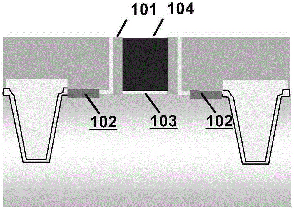
[0049] Embodiments of the present invention are described in detail below, examples of which are shown in the drawings, wherein the same or similar reference numerals designate the same or similar elements or elements having the same or similar functions throughout. The embodiments described below by referring to the figures are exemplary only for explaining the present invention and should not be construed as limiting the present invention. Furthermore, the present invention may repeat reference numerals and / or letters in different instances. This repetition is for the purpose of simplicity and clarity and does not in itself indicate a relationship between the various embodiments and / or arrangements discussed.

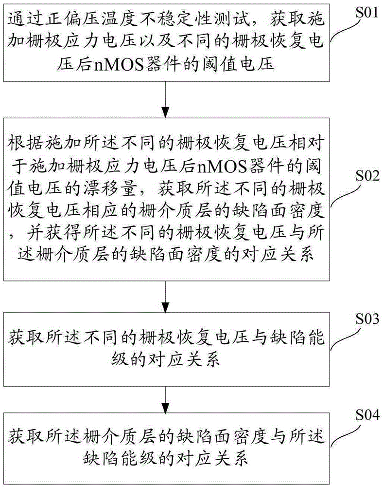
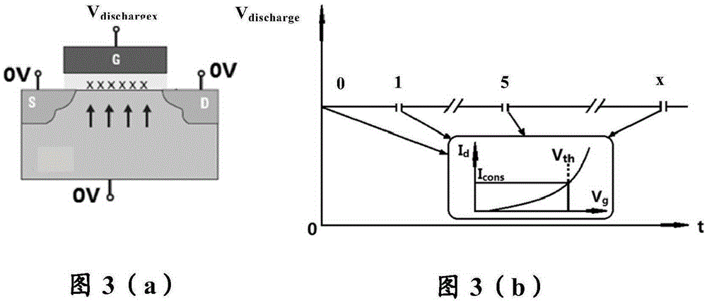
[0050] The method for extracting semiconductor defect energy levels provided by the present invention obtains the drift amount of the threshold voltage of the nMOS device after applying different gate recovery voltages through the positive bias temperature instability t...


PUM


Abstract

The invention provides a method and a system for extracting a semiconductor defect level. The method comprises steps: through a positive bias temperature instability test, the threshold voltage of an nMOS device after applying gate stress voltage and different gate recovery voltage is acquired; according to the shift of the threshold voltage of the nMOS device after applying the different gate recovery voltage relative to applying the gate stress voltage, the defect surface density of a gate dielectric layer corresponding to the different gate recovery voltage is acquired, and the corresponding relationship between the different gate recovery voltage and the defect surface density of the gate dielectric layer is acquired; the corresponding relationship between the different gate recovery voltage and a defect level is acquired; and the corresponding relationship between the defect surface density of the gate dielectric layer and the defect level is acquired. According to the method provided by the invention, the relationship between the defect level and the defect surface density of the gate dielectric layer can be extracted, and the device performance and the reliability can be improved.

Description

technical field [0001] The invention relates to the field of semiconductor manufacturing, in particular to a method and system for extracting semiconductor defect energy levels. Background technique [0002] As the process nodes of semiconductor chips continue to decrease, the thickness of the gate oxide layer becomes thinner and thinner, and the reliability of the device is paid more and more attention; in addition, with the introduction of the gate oxide nitride process, the reliability of the device is particularly important. The Bias Temperature Instability (BTI) effect occupies the primary position in the reliability of the device. The BTI effect means that when a certain gate voltage is applied to the gate of the field effect transistor MOSFET, the performance of the device will occur under high temperature stress conditions. Significant degradation and reduced device lifetime are mainly manifested in the drift of threshold voltage, the drop of drive current and transc...

Claims


Application Information

Patent Timeline
Patent Type & Authority Applications(China)
IPC IPC(8): G01R31/26
CPCG01R31/2601
Inventor 祁路伟任尚清杨红
Owner INST OF MICROELECTRONICS CHINESE ACAD OF SCI
Why Eureka
Try Eureka