Intelligent screen pasting film and preparing method thereof
A technology of smart stickers and screens, applied in instruments, electrical digital data processing, packaging, etc., can solve problems such as failure, affecting operation experience, blocking touch icons or touch points, etc., to improve product reliability and excellent flexibility , good user experience effect
- Summary
- Abstract
- Description
- Claims
- Application Information
AI Technical Summary
Problems solved by technology
Method used
Image


Examples
Embodiment 1
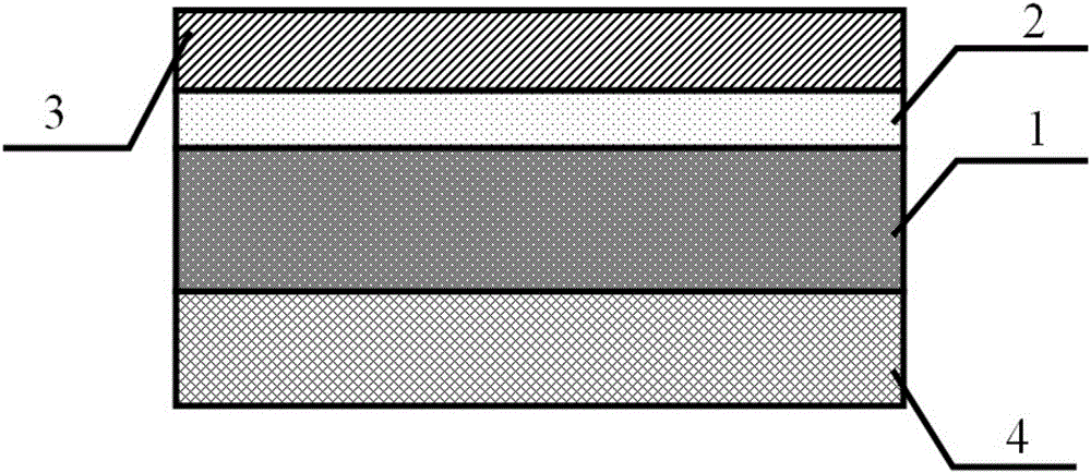
[0059] A kind of intelligent protective film and manufacturing method, see image 3 , including the following steps:
[0060] (1) on the back side of the anti-fingerprint coating of anti-fingerprint PET film 3, utilize electrostatic transfer method to transfer graphene 5, and the number of layers of graphene is single-layer or double-layer;
[0061] (2) Adopt the technology of laser direct writing etching, carry out laser etching process to the graphene 5 that step (1) forms, directly form the pattern of graphene transparent conductive film, patterned shape sees Figure 5 As shown, it includes a touch area 51 and a trigger area 52, the touch area 51 and the trigger area 52 are connected by a conductive area 53, and the left and right patterned graphene patterns can only be set on the left or right, or can be set at the same time;
[0062] (3) fit the AB adhesive layer 4 so that one side of the AB glue acrylate adhesive 41 is fitted with the graphene 5 sides;
[0063] (4) Car...
Embodiment 2
[0067] A kind of intelligent protective film and manufacturing method, see image 3 , including the following steps:
[0068] (1) on the anti-fingerprint coating backside of the anti-fingerprint PET film 3, utilize the adhesive method to transfer graphene 5, and the number of graphene layers is a single layer;
[0069] (2) Adopt yellow light method etching process, the graphene 5 that step (1) forms is carried out etching process, directly form the pattern of graphene transparent conductive film, patterned shape sees Figure 5 As shown, it includes a touch area 51 and a trigger area 52, the touch area 51 and the trigger area 52 are connected by a conductive area 53, and the left and right patterned graphene patterns can only be set on the left or right, or can be set at the same time;
[0070] (3) fit the AB adhesive layer 4 so that one side of the AB glue acrylate adhesive 41 is bonded with the graphene 5;
[0071] (4) Carry out laser cutting or punching on the complete str...
Embodiment 3
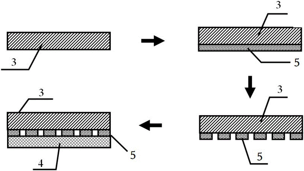
[0075] A kind of optimized intelligent protective film and manufacturing method, see Figure 4 , including the following steps:
[0076] (1) on the anti-fingerprint coating backside of anti-fingerprint PET film 3, utilize electrostatic transfer method to transfer graphene 5, and the number of layers of graphene is single-layer or double-layer;
[0077] (2) Lay the AB adhesive layer 4 so that one side of the AB adhesive layer acrylate adhesive 41 (see figure 2 ) is bonded with graphene 5 to protect the graphene film;
[0078] (3) Adopt laser direct writing etching process, on the anti-fingerprint film surface, carry out laser etching process to the graphene film formed in step (2) through the anti-fingerprint film, directly form the pattern of graphene transparent conductive film, pattern see Figure 5 As shown, it includes a touch area 51 and a trigger area 52, the touch area 51 and the trigger area 52 are connected by a conductive area 53, and the left and right patterned...
PUM
| Property | Measurement | Unit |
|---|---|---|
| Thickness | aaaaa | aaaaa |
| Width | aaaaa | aaaaa |
| Thickness | aaaaa | aaaaa |
Abstract
Description
Claims
Application Information
 - R&D
- Intellectual Property
- Life Sciences
- Materials
- Tech Scout
- Unparalleled Data Quality
- Higher Quality Content
- 60% Fewer Hallucinations
Browse by: Latest US Patents, China's latest patents, Technical Efficacy Thesaurus, Application Domain, Technology Topic, Popular Technical Reports.
© 2025 PatSnap. All rights reserved.Legal|Privacy policy|Modern Slavery Act Transparency Statement|Sitemap|About US| Contact US: help@patsnap.com