Ultraviolet LED encapsulation method
A technology of LED packaging and LED chips, applied in semiconductor devices, electrical components, circuits, etc., can solve the problems of affecting chip performance, easy aging of materials, loss of sealing performance, etc., to achieve uniform protective film, improve cleanliness, and prolong sealing time. Effect
- Summary
- Abstract
- Description
- Claims
- Application Information
AI Technical Summary
Problems solved by technology
Method used
Image

Examples
Example Embodiment
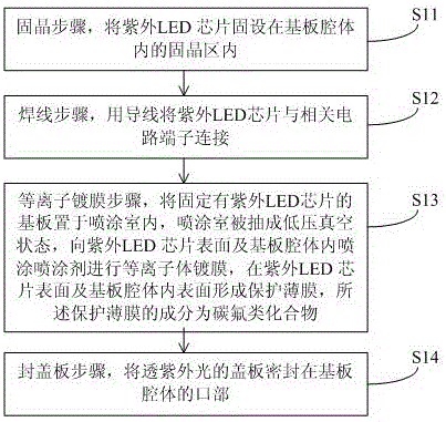
[0033] Example one
[0034] This embodiment proposes a UV LED packaging method, such as figure 1 As shown, including the following steps:
[0035] S11. In the die bonding step, the ultraviolet LED chip is secured in the die bonding area in the substrate cavity;
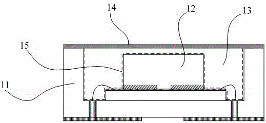
[0036] This embodiment uses the chip-on-board packaging technology, such as figure 2 As shown, a substrate 11 is included. The substrate 11 has a cavity 13 for accommodating the chip 12.
[0037] S12, the wire bonding step, connect the ultraviolet LED chip with the relevant circuit terminal with a wire;
[0038] S13. Plasma coating step: place the substrate with the UV LED chip fixed in the spraying chamber, and the spraying chamber is drawn into a low-pressure vacuum state, and spraying agent is sprayed on the surface of the UV LED chip and the substrate cavity for plasma coating, on the surface of the UV LED chip And the inner surface of the substrate cavity to form a protective film, the composition of the protective film ...
Example Embodiment
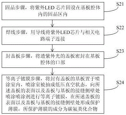
[0048] Example two
[0049] This embodiment proposes another UV LED packaging method, such as image 3 As shown, including the following steps:
[0050] S21, the die bonding step, fixing the ultraviolet LED chip in the die bonding area in the substrate cavity;
[0051] This embodiment adopts the chip-on-board packaging technology, such as Figure 4 As shown, a substrate 11 is included. The substrate 11 has a cavity 13 for accommodating the chip 12.
[0052] S22, the wire bonding step, connect the ultraviolet LED chip with the relevant circuit terminal with a wire;
[0053] S23. The step of sealing the cover plate, sealing the cover plate which transmits ultraviolet light on the mouth of the substrate cavity.
[0054] S24. Plasma coating step: place the substrate with the cover plate in the spraying chamber, and the spraying chamber is evacuated into a low-pressure vacuum state, and spraying agent is sprayed on the surface of the cover plate and the side wall of the joint between the cov...
PUM
| Property | Measurement | Unit |
|---|---|---|
| Thickness | aaaaa | aaaaa |
| Heat resistant | aaaaa | aaaaa |
Abstract
Description
Claims
Application Information
 - R&D
- Intellectual Property
- Life Sciences
- Materials
- Tech Scout
- Unparalleled Data Quality
- Higher Quality Content
- 60% Fewer Hallucinations
Browse by: Latest US Patents, China's latest patents, Technical Efficacy Thesaurus, Application Domain, Technology Topic, Popular Technical Reports.
© 2025 PatSnap. All rights reserved.Legal|Privacy policy|Modern Slavery Act Transparency Statement|Sitemap|About US| Contact US: help@patsnap.com