A Method for Improving the Oxidation Resistance of nb-Si-Based Alloys Using Electron Beam Remelting Technology
A technology of electron beam remelting and oxidation resistance, which is applied in the field of improving the oxidation resistance of Nb-Si-based alloys by using electron beam surface remelting technology, can solve the problems of insufficient high-temperature oxidation performance of Nb-Si-based alloys, and achieve improved high-temperature Oxidation resistance, effect of improving high temperature oxidation resistance
- Summary
- Abstract
- Description
- Claims
- Application Information
AI Technical Summary
Problems solved by technology
Method used
Image
Examples
Embodiment 1
[0031] 1. Using high-purity Nb and Si as synthetic raw materials, the Nb-20Si alloy master ingot was obtained by arc melting technology, and a circular substrate with a diameter of 60mm and a thickness of 15mm was cut by wire cutting, and the surface of the sample was polished, cleaned and dried spare;
[0032] 2. Fix the Nb-20Si alloy substrate on the workbench, and pump the sealed forming cavity into a high vacuum state;
[0033] 3. Preheat the Nb-20Si alloy substrate with a high-energy electron beam. The preheating temperature is 900°C. The specific preheating parameters are: accelerating voltage 30kV, current 9.0mA, and electron beam focal spot size 100μm;
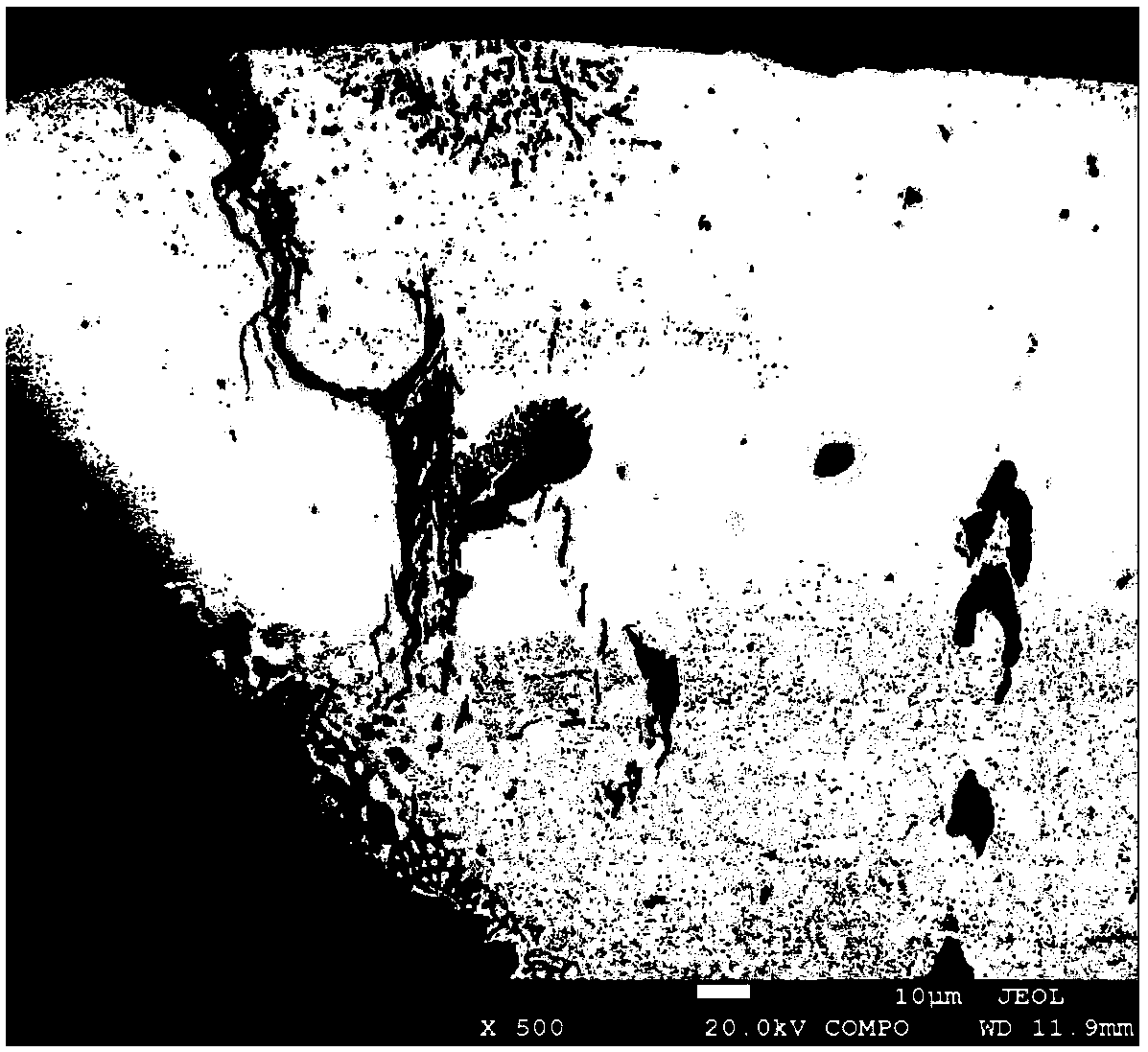
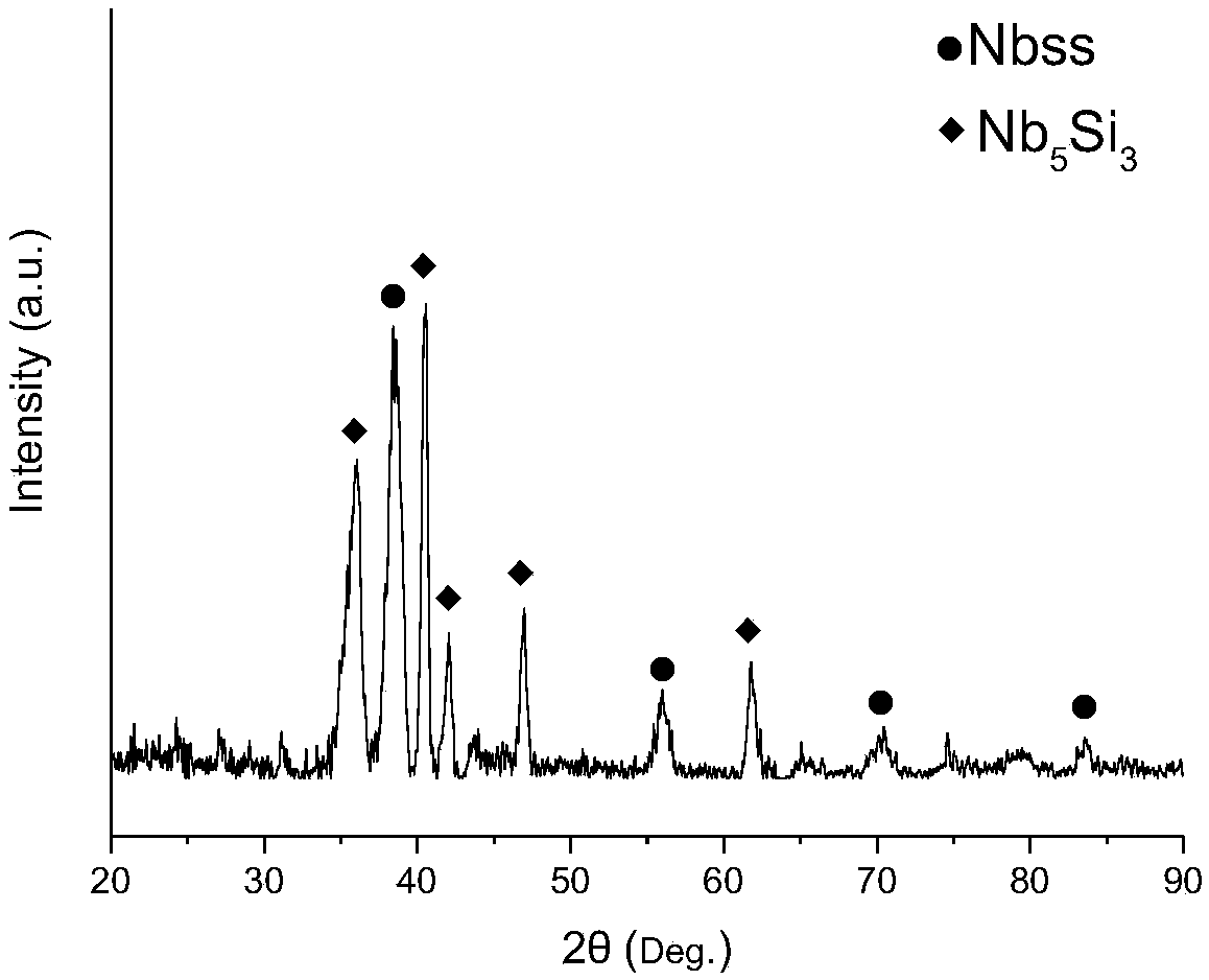
[0034] 4. After the preheating is over, set the corresponding processing parameters, scan the surface of the Nb-20Si alloy substrate with an electron beam, the surface of the sample is melted and solidified, and a remelting layer is formed. The specific remelting parameters: accelerating voltage 30kV, scanning current ...
Embodiment 2
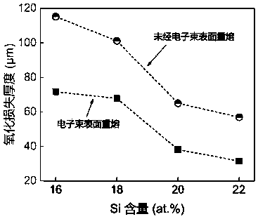
[0037]1. Using high-purity Nb, Si, Ti, Cr, and Al as synthetic raw materials, four kinds of Nb-Si-based alloy master ingots were obtained by vacuum induction melting technology. The alloy components were Nb-16Si-24Ti-2Cr-2Al, Nb- 18Si-24Ti-2Cr-2Al, Nb-20Si-24Ti-2Cr-2Al, Nb-22Si-24Ti-2Cr-2Al, using wire cutting to cut the circular substrates of the four alloys, with a diameter of 70mm and a thickness of 15mm, and the samples The surface is polished, cleaned and dried for later use;
[0038] 2. Fix the four alloy substrates on the workbench at the same time, and pump the sealed forming cavity into a high vacuum state;
[0039] 3. Use high-energy electron beams to preheat four kinds of Nb-Si alloy substrates. The preheating temperature is 1200°C. The specific preheating parameters are: accelerating voltage 30kV, scanning current 20mA, and electron beam focal spot size 100μm;
[0040] 4. After the preheating is over, set the corresponding processing parameters, and scan the surfa...
PUM
| Property | Measurement | Unit |
|---|---|---|
| thickness | aaaaa | aaaaa |
| thickness | aaaaa | aaaaa |
| thickness | aaaaa | aaaaa |
Abstract
Description
Claims
Application Information
 - R&D
- Intellectual Property
- Life Sciences
- Materials
- Tech Scout
- Unparalleled Data Quality
- Higher Quality Content
- 60% Fewer Hallucinations
Browse by: Latest US Patents, China's latest patents, Technical Efficacy Thesaurus, Application Domain, Technology Topic, Popular Technical Reports.
© 2025 PatSnap. All rights reserved.Legal|Privacy policy|Modern Slavery Act Transparency Statement|Sitemap|About US| Contact US: help@patsnap.com


