PCB warpage leveling method with independent lines and pads

A PCB board and soldering pad technology, applied in the field of PCB warping and leveling, can solve problems such as board surface solder mask peeling off, increase manufacturing costs, and fail to meet customer requirements, and achieve the effect of solving board warping reduction and ensuring product quality

Inactive Publication Date: 2019-07-26
SHENZHEN CHENGHE ELECTRONICS IND
View PDF3 Cites 0 Cited by
  • Summary
  • Abstract
  • Description
  • Claims
  • Application Information

AI Technical Summary

Problems solved by technology

At present, for PCBs with only a small number of independent lines and pads designed on the entire board, after the entire PCB electroplating process, the independent lines and pads are not on the horizontal plane with the board surface, and are more prominent than the board surface. Therefore, When the PCB is stacked before the pressing board, there are independent lines and independent lines, pads and pads, and independent lines and pads superimposed between adjacent PCBs. There are phenomena such as solder mask peeling off on the independent line of the board or marks on the independent pad and independent circuit pressure plate, which leads to poor appearance of the finished PCB and cannot meet customer requirements, which greatly increases the manufacturing cost and is not conducive to the development of the enterprise.
In order to solve the above problems, the prior art usually adopts the method of manually warping the board, but the disadvantage of this method is that the stress on the board surface is not completely eliminated after the board is warped, and there is a hidden danger of board warping restoration

Method used


Image

  • PCB warpage leveling method with independent lines and pads
  • PCB warpage leveling method with independent lines and pads
  • PCB warpage leveling method with independent lines and pads

Examples


Embodiment Construction

[0030] In order to make the object, technical solution and advantages of the present invention clearer, the present invention will be further described in detail below in conjunction with the accompanying drawings and embodiments. It should be understood that the specific embodiments described here are only used to explain the present invention, not to limit the present invention.

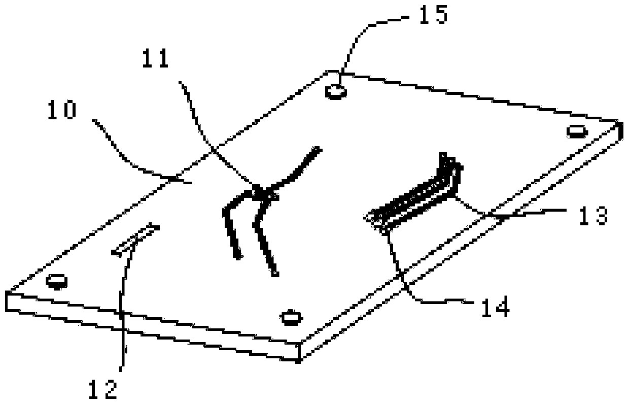
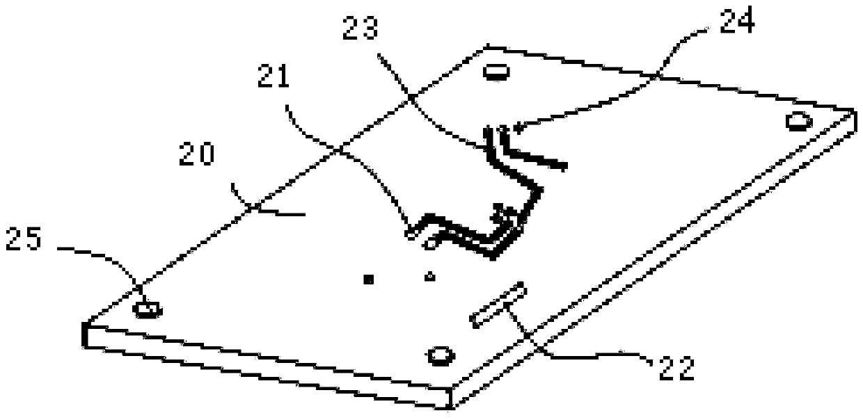
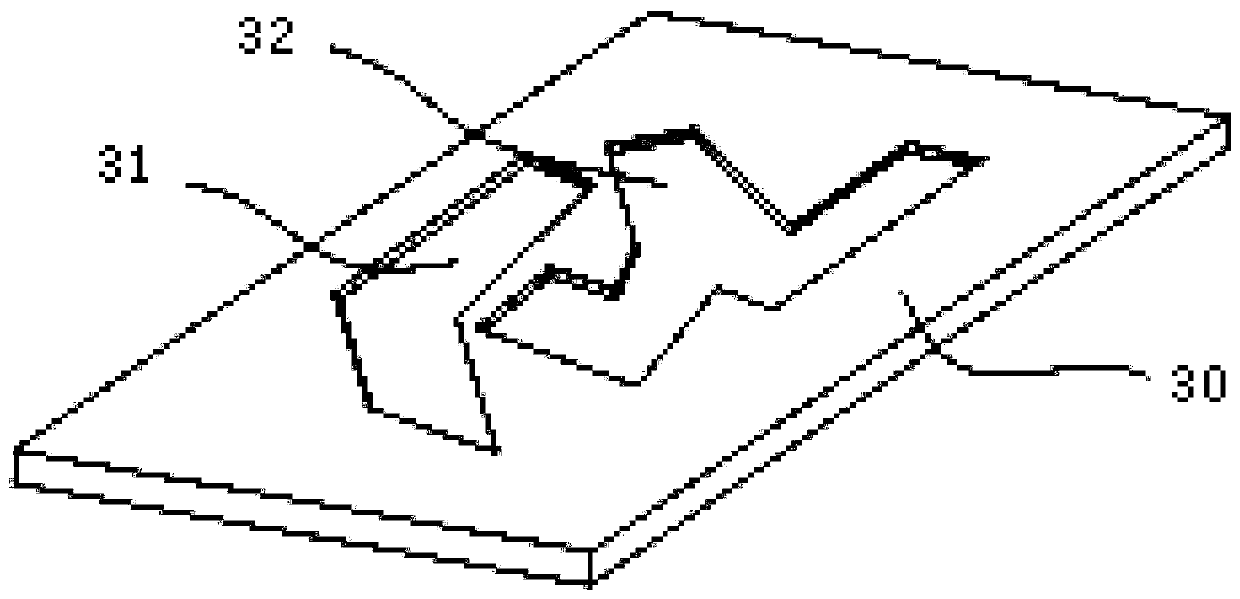
[0031] For some PCB boards with independent lines and pads and the board surface that are not on the horizontal plane, the PCB stress cannot be completely eliminated by manual punching, resulting in the problem of board warpage reduction. The present invention proposes a PCB warping and leveling method with independent lines and solder pads, which adds a backing plate between two adjacent finished PCB boards, and makes the lines, holes, and interiors on the finished PCB boards The grooves and pads fall into the through grooves and hang in the air, so as to avoid the poor appearance caused by the di...


PUM


Abstract

The present invention provides a PCB warping leveling method with independent lines and pads. A base plate is arranged between two adjacent finished product PCBs, a straight slot is correspondingly arranged on the base plate according to the line, the hole, the internal groove and the pads at two surfaces of the finished product PCBs to allow the line, the hole, the internal groove and the pads to be correspondingly located in the straight slot at pressing the plate so as to avoid the problem that the appearance is not good caused by directly contacting a bump-cutter machine with the finished product PCBs when pressing the plate. Compared to the prior art, the hidden trouble can be solved that the manual work plate pressing warping PCB stress is not completely eliminated to cause the recovery of the plate warping, and the product quality is ensured.

Description

technical field [0001] The invention relates to the technical field of printed circuit board manufacturing, in particular to a PCB warpage leveling method with independent circuits and pads. Background technique [0002] PCB is the carrier of electrical connection of electronic components. With the multi-functional development of PCB, the circuit layout and design are different. There are multiple BGA and IC integrated designs for the whole board, and there are also independent circuit and pad designs for the whole board. [0003] As electronic terminals have higher and higher requirements for PCB assembly, in order to ensure the warping reliability of the finished PCB, a leveler is required to level the plate before shipment. At present, for PCBs with only a small number of independent lines and pads designed on the entire board, after the entire PCB electroplating process, the independent lines and pads are not on the horizontal plane with the board surface, and are more ...

Claims


Application Information

Patent Timeline
Patent Type & Authority Patents(China)
IPC IPC(8): H05K3/00
CPCH05K3/0014H05K2203/0278
Inventor 杜景强
Owner SHENZHEN CHENGHE ELECTRONICS IND
Why Eureka
Try Eureka