Composite electronic component and preparation method thereof
A technology of electronic components and electrode layers, applied in electrical components, circuits, capacitors, etc., can solve problems such as unfavorable miniaturization of the whole machine, multiple circuit spaces, and low mounting efficiency.
- Summary
- Abstract
- Description
- Claims
- Application Information
AI Technical Summary
Problems solved by technology
Method used
Image
Examples
preparation example Construction
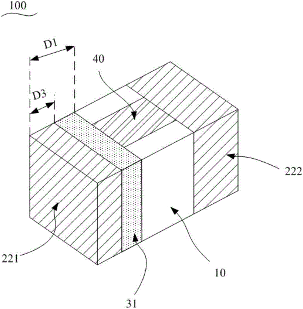
[0069] The flowchart of the preparation method of the composite electronic component of one embodiment is as follows Figure 12 As shown, the following steps S110-S150 are included.
[0070] S110, providing a ceramic body.
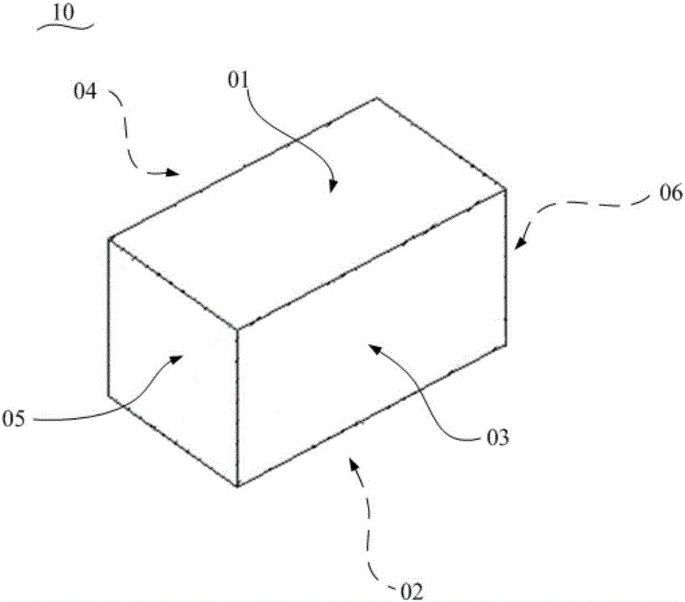
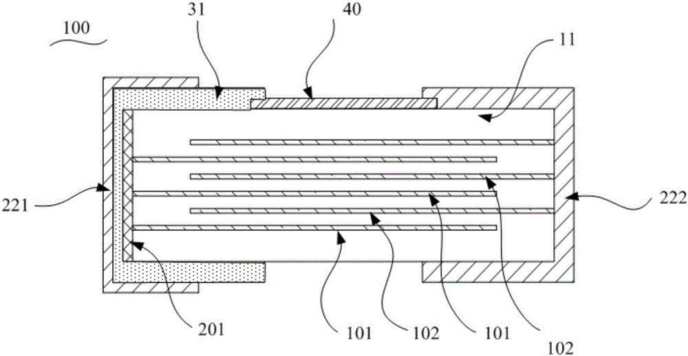
[0071] Wherein, the ceramic body is a cuboid, and the ceramic body has a first end surface and a second end surface opposite to each other, and four side surfaces connecting the first end surface and the second end surface. The inside of the ceramic body is filled with a ceramic medium, and a plurality of first electrode layers and a plurality of second electrode layers are interspersed in the ceramic medium, and the first electrode layers and the second electrode layers are alternately stacked, and the first electrode layers are on the second electrode layers The projection of and the second electrode layer overlap, and the space between the first electrode layer and the second electrode layer is filled with a ceramic medium. At least one part of the fi...
Embodiment 1
[0122] Preparation of composite electronic components
[0123] 1) Preparation of a ceramic body: ceramic powder, a binder and an organic solvent are mixed to obtain a ceramic slurry, and a plurality of ceramic dielectric films are formed by casting the ceramic slurry as a raw material. Wherein, the ceramic slurry includes 10 parts of ceramic powder, 4 parts of binder and 5 parts of organic solvent in parts by mass. The ceramic powder is barium titanate ceramics, the binder is polyvinyl butyral, and the organic solvent is a mixed solvent of toluene and ethanol with a ratio of parts by mass of 1:1. The electrode paste is printed on a plurality of ceramic dielectric films to respectively obtain a ceramic dielectric film printed with a first electrode layer and a ceramic dielectric film printed with a second electrode layer. The screen pattern of the first electrode layer and the second electrode layer is as Figure 15 As shown, the shaded part indicates where the electrode past...
Embodiment 2
[0130] The preparation method of the composite electronic component of this embodiment is similar to that of Embodiment 1, except that it further includes coating an electrode paste on the second end surface of the ceramic body to form a second connecting electrode. Then, the resistance paste is dipped on the second end surface covered with the second connection electrode to obtain a second resistance layer, and the second resistance layer and the surface electrode have overlapping portions. Then cover the electrode paste on the second resistance layer to form a second terminal electrode.
[0131] The specific structure of the composite electronic component of this embodiment is as Figure 7 ~ Figure 10 As shown, the equivalent circuit is as Figure 11 shown.
PUM
 Abstract
Description
Claims
Application Information
 - R&D
- Intellectual Property
- Life Sciences
- Materials
- Tech Scout
- Unparalleled Data Quality
- Higher Quality Content
- 60% Fewer Hallucinations
Browse by: Latest US Patents, China's latest patents, Technical Efficacy Thesaurus, Application Domain, Technology Topic, Popular Technical Reports.
© 2025 PatSnap. All rights reserved.Legal|Privacy policy|Modern Slavery Act Transparency Statement|Sitemap|About US| Contact US: help@patsnap.com


