Micro-nano structure inscribing device based on sample rotation and laser double-beam interference
A double-beam interference, micro-nano structure technology, which is applied in photolithography process exposure devices, microlithography exposure equipment, optics, etc., can solve the problems of inconvenient operation, high price, complicated optical path, etc. Easy to operate, simple light path effect
- Summary
- Abstract
- Description
- Claims
- Application Information
AI Technical Summary
Problems solved by technology
Method used
Image
Examples
Embodiment 1
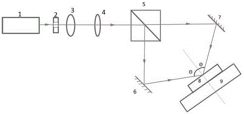
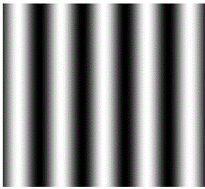
[0034] refer to figure 1 The structure diagram of a micro-nano structure writing device based on sample rotation and laser double-beam interference is shown. The He-Cd laser source 1 selects the laser beam with an emission wave of 325nm, opens the photoelectric shutter 2, and the laser beam passes through the photoelectric shutter 2. , after passing through the short focal length lens 3 and the long focal length lens 4, the beam is expanded, and then divided into two beams of coherent light with the same intensity by the beam splitter 5, emitted from two directions, and finally reflected by the plane reflector A6 and the plane reflector B7 To expose it on the photoresist sample 8, the incident angle θ =10°, after exposure for a certain period of time, a one-dimensional periodic grating structure can be obtained through subsequent developing, fixing and other processes. Such as image 3 shown.
Embodiment 2
[0036] refer to figure 1 Shown is a schematic structural diagram of a micro-nano structure writing device based on sample rotation and laser double-beam interference. After the first exposure of the sample with a 325nm laser beam for a certain period of time, the photoelectric shutter 2 is closed, and the photolithographic process is performed through the sample rotation system 9. The glue sample 8 is rotated 90°, and then the photoelectric shutter 2 is opened to expose the photoresist sample 8 again for the same time T , refer to Example 1 for other steps, the finally obtained micro-nano structure is a two-dimensional periodic lattice structure, such as Figure 4 shown.
Embodiment 3
[0038] refer to figure 1 Shown is a schematic structural diagram of a micro-nano structure writing device based on sample rotation and laser double-beam interference. The photoresist sample 8 is exposed three times, and the photoelectric shutter 2 is closed after each exposure for the same time, and the sample rotation controller 9 enables The photoresist sample 8 is rotated by 60°, and other steps refer to Example 1 to obtain a hexagonal lattice structure, such as Figure 5 shown.
PUM
 Abstract
Description
Claims
Application Information
 - R&D
- Intellectual Property
- Life Sciences
- Materials
- Tech Scout
- Unparalleled Data Quality
- Higher Quality Content
- 60% Fewer Hallucinations
Browse by: Latest US Patents, China's latest patents, Technical Efficacy Thesaurus, Application Domain, Technology Topic, Popular Technical Reports.
© 2025 PatSnap. All rights reserved.Legal|Privacy policy|Modern Slavery Act Transparency Statement|Sitemap|About US| Contact US: help@patsnap.com


