
An Integrated Surface Plasmonic Logic Circuit

A surface plasmon and logic technology, applied in logic circuits, logic circuits using specific components, logic circuits using optoelectronic devices, etc. Output signal stability and other issues to achieve the effect of reducing cost and difficulty, small size, and long transmission distance

Inactive Publication Date: 2019-08-09
BEIJING NORMAL UNIVERSITY
View PDF6 Cites 0 Cited by
  • Summary
  • Abstract
  • Description
  • Claims
  • Application Information

AI Technical Summary

Problems solved by technology

Recently, the design of all-optical logic gates based on surface plasmons has also been reported frequently, but there are still some limitations, such as the use of silver nanowires mentioned in dx.doi.org / 10.1021 / nl103228b (NanoLett.2011, 11, 471–475) The surface-propagated plasmon interference logic gate is limited by the length and high loss of silver nanowires. The propagation length of surface plasmons is less than 20um. The specific gate structure requires precise input signal polarization angles, which reduces the stability of the output signal; based on The optical logic gate dx.doi.org / 10.1021 / nl303095s (Nano Lett.2012,12,5784-5790) of the metal groove waveguide, due to the large loss of the waveguide arc design, the surface plasmon propagation distance is short and the output signal strength The contrast ratio is small, and the small waveguide width makes dust and small particles in the air have a great impact on the waveguide performance

Method used


Image

  • An Integrated Surface Plasmonic Logic Circuit
  • An Integrated Surface Plasmonic Logic Circuit
  • An Integrated Surface Plasmonic Logic Circuit

Examples


Embodiment 1

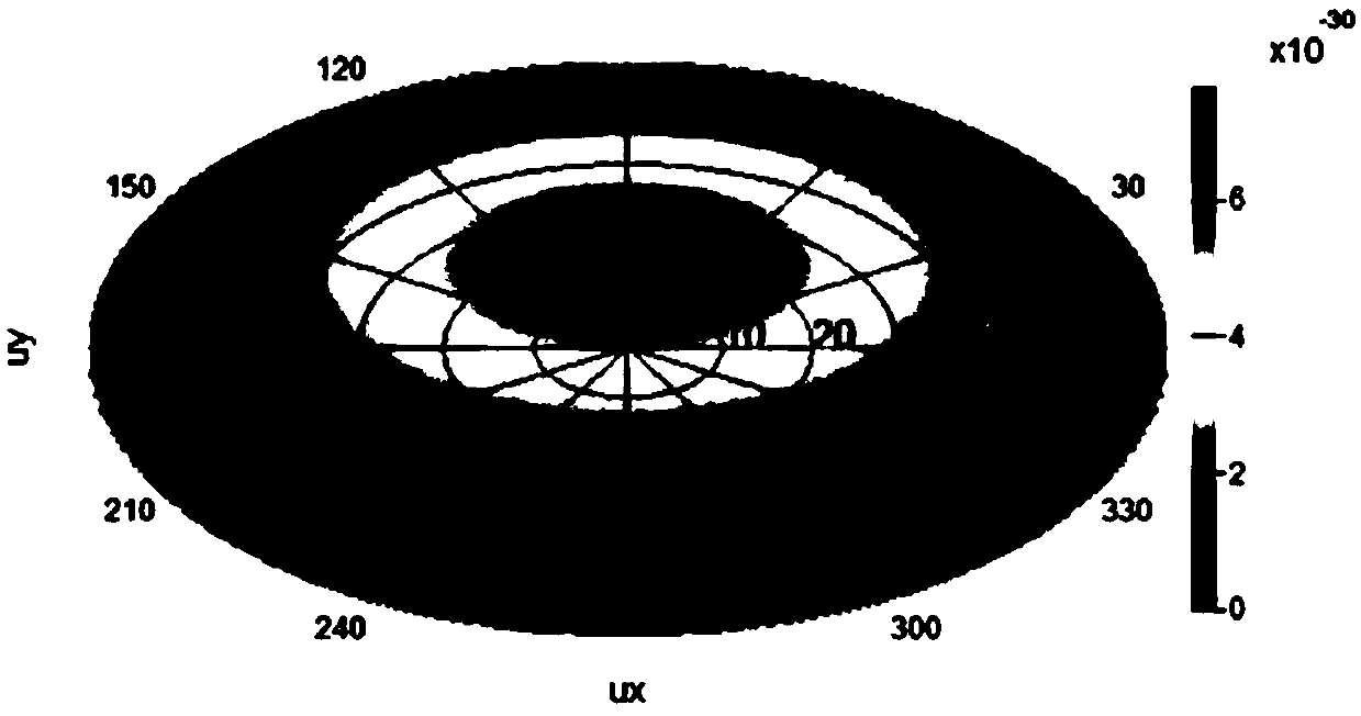
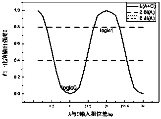
[0028] Fig. 2 shows the simulated light intensity distribution diagram of the "AND" logic gate of the present invention. The working principle is as follows: Two beams of coherent light are respectively injected from the input terminal A and input terminal C, after passing through the Fresnel zone plate, they converge at the output terminal D and perform interference calculation, and are detected by the optical power meter placed here at the same time light intensity. Since the coupling coefficient of the coupled output grating or slit is different due to the manufacturing process, for each specific device, a normalized intensity spectrum is defined. When all the components participating in the interference are in the same phase, the output intensity is the strongest, which is defined as normalized Intensity 1, defined as normalized intensity 0 when completely interfering and destructive. For the input terminal, it is defined as logic "1" when there is light injection, and log...

Embodiment 2

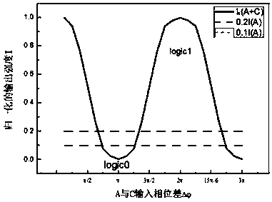
[0031] The working principle is the same as that of Embodiment 1. Table 1 shows the optical logic operation results of the "OR" gate. Unlike the "AND" gate, the threshold value of the "OR" gate is changed. When doing "OR" logic gate operation, for the output terminal, according to the normalized intensity spectrum, the optical power greater than 0.2 is defined as logic "1", and less than 0.1 is defined as logic "0", such as image 3 As shown, this threshold is defined as "Threshold 2". According to the result of optical logic operation and the definition of "threshold", Table 2 gives the corresponding truth table, which reflects the logical relationship of "OR" between input terminal A and input terminal C, and realizes the function of "OR" logic gate.

Embodiment 3

[0033] The working principle is the same as that of Embodiment 1 and the definition of "threshold 2" is adopted. Table 1 shows the result of the "exclusive OR" optical logic operation and the corresponding truth table. Among them, "-I" and "I" indicate that the light intensity is the same, but the phase difference is "π". The truth table reflects the "exclusive OR" logic relationship between the input terminal A and the input terminal C, and realizes the function of the "exclusive OR" logic gate.


PUM


Abstract

The invention relates to an integration type full-optical logic gate device and logic operation method thereof based on surface plasmon. The integration type full-optical logic gate device and logic operation method thereof based on surface Plasmon are characterized in that the full-optical logic gate device comprises an input module, an SPP convergence module and an output module. The input module is a three-input gate structure, and the three-input structure is composed of three groups of optical gratings which are of equal structures and are distributed equally and horizontally, that is, an input port A, a control port B and an input port C. When only dual-input ports are needed, the control port B can be left unused; the SPP convergence module comprises wave zone plates under a non-paraxial condition; the output module comprises an output end and an optical detector. The integration type surface plasmon logic circuit realizes a pure optic logic operation, compared with the prior art, the integration type surface plasmon logic circuit is high in integration level, small in volume, low in signal light consumption, far in transmission distance and has a potential of multi-level cascade; meanwhile, the integration type surface plasmon logic circuit covers lights of all wave length ranging from near ultraviolet to intermediate infrared, with 1.55 um communication wave length included.

Description

technical field [0001] The invention relates to an optical logic gate device for realizing all-optical logic operations on light wave signals, which is applied in the fields of optical communication, all-optical computing, and integrated optical circuits, and in particular to an ultra-small integrated all-optical logic gate device based on surface plasmons Optical logic gate device and its logic operation method. Background technique [0002] Traditional optical communication systems have problems such as bulky, complex structures, and high energy consumption, which have been difficult to meet the rapid development of communication needs. The development of all-optical technology is an important basis for the realization of future communication networks. All-optical logic gates are the basic unit in optical signal processing and the key components to realize optical packet switching, optical computing and future high-speed and large-capacity optical networks. At present, ma...

Claims


Application Information

Patent Timeline
Patent Type & Authority Patents(China)
IPC IPC(8): G02F3/00
CPCG02F3/00
Inventor 石锦卫武晓佳桑云刚丁宇峰王艳容郭华清周静刘大禾
Owner BEIJING NORMAL UNIVERSITY
Learn More