Lighting device, display device and television receiver

Inactive Publication Date: 2012-04-12
SHARP KK
View PDF16 Cites 60 Cited by
  • Summary
  • Abstract
  • Description
  • Claims
  • Application Information

AI Technical Summary

Benefits of technology

[0008]The present invention was accomplished in view of the above circumstances. It is an object of the present invention to provide a lighting device realizing cost reduction, suppressing of power consumption, and suppressing lamp image generation. It is another object of the present invention to provide a display device including the lighting device. It is still another object of the present invention to provide a television receiver including the display device.Means for Solving the Problem
[0010]Thus, the point light sources are arranged such that the light source high-density area and the light source low-density area are provided. Thereby, the number of the point light sources can be reduced as compared with a case where the light source high-density area is formed over the entire chassis, to realize cost reduction and power saving. Because a distance between the point light sources that are adjacent to each other in the light source low-density area is comparatively larger when the light source low-density area is formed, light emitted from the point light sources is likely to reach the optical member without mixing the light with each other. As a result, brightness in a region overlapping with the point light sources in the optical member is locally increased, which tends to generate a lamp image. Then, in the present invention, the optical member has the light reflection portion reflecting light from each point light source formed in at least the region overlapping with the light source low-density area. Thereby, the light emitted from the point light sources in the light source low-density area is mostly reflected to the chassis side by the light reflection portion once. The light is reflected in the chassis while the light is mixed with each other, and can reach the optical member again. Thereby, almost uniform brightness can be obtained over the entire optical member, and the generation of the lamp image can be suppressed.

Problems solved by technology

However, when the point-like light is not sufficiently converted into the planar light, a point lamp image is generated along arrangement of the light sources, which deteriorates display quality of the liquid crystal display device.
However, when the number of the light sources is increased, cost of the backlight unit is increased, and power consumption is also increased.
When the diffusivity of the diffuser is increased, brightness cannot be increased, which disadvantageously requires an increase in the number of the light sources at the same time.

Method used


Image

  • Lighting device, display device and television receiver
  • Lighting device, display device and television receiver
  • Lighting device, display device and television receiver

Examples


first embodiment

Modification of First Embodiment

[0058]As described above, the first embodiment of the present invention has been illustrated. However, the present invention is not limited to the above embodiment. A modification of a distribution mode of the light reflection portions 50 illustrated in FIG. 7 may be employed, for example. In this modification, the same constituent parts and constituent elements as those of the first embodiment are indicated by the same symbols, and will not be described.

[0059]The diffuser 15a in the present modification includes at least the light reflection portions 50 provided in positions facing the LED light sources 80 in not only the position overlapping with the light source low-density area LL but also the position overlapping with the light source high-density area LH as illustrated in FIG. 7. In this case, in the light reflection portions 50, the area of the dot in the position overlapping with the light source high-density area LH is smaller than the area i...

second embodiment

[0061]Next, a second embodiment of the present invention will be described with reference to FIGS. 9 to 11.

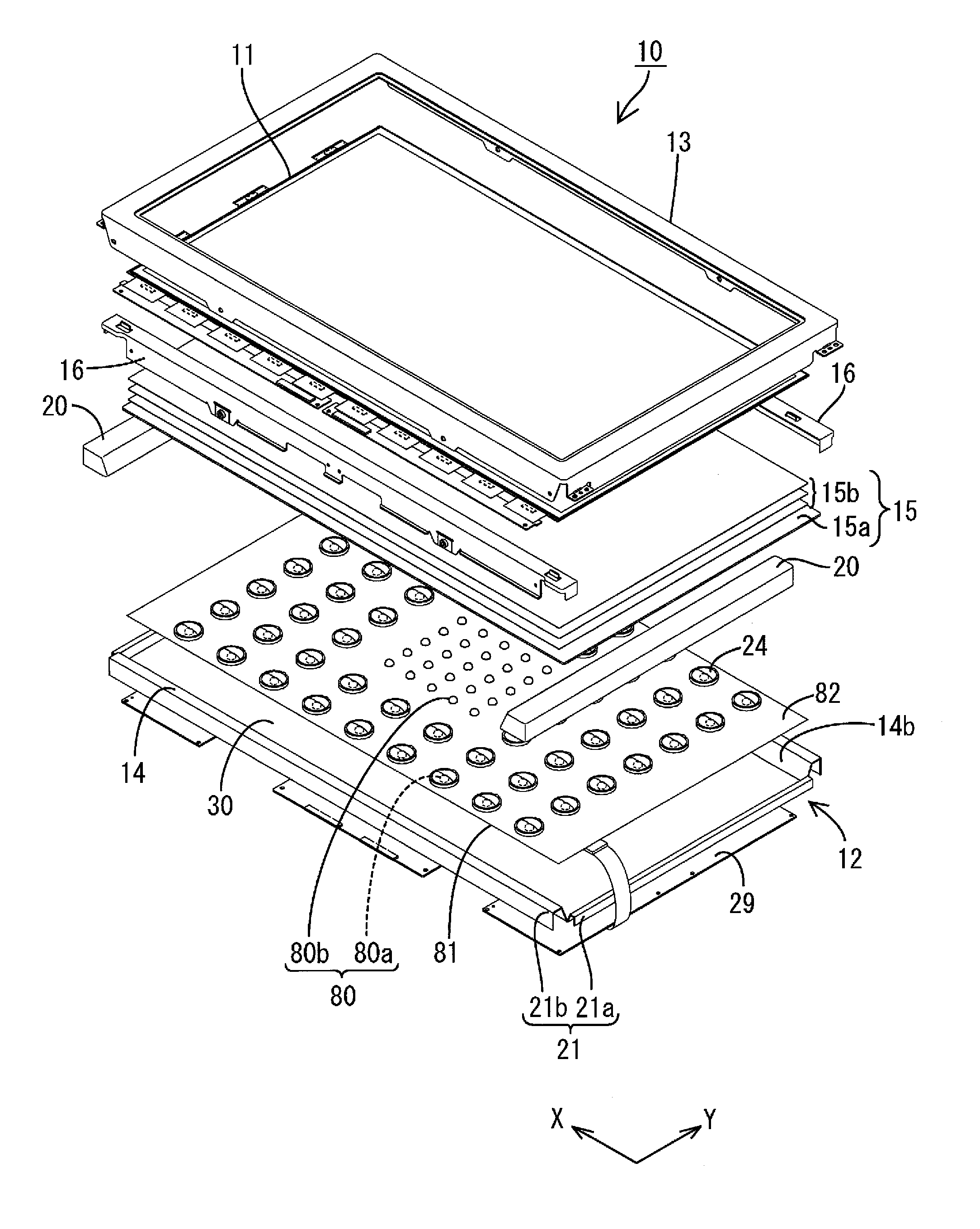
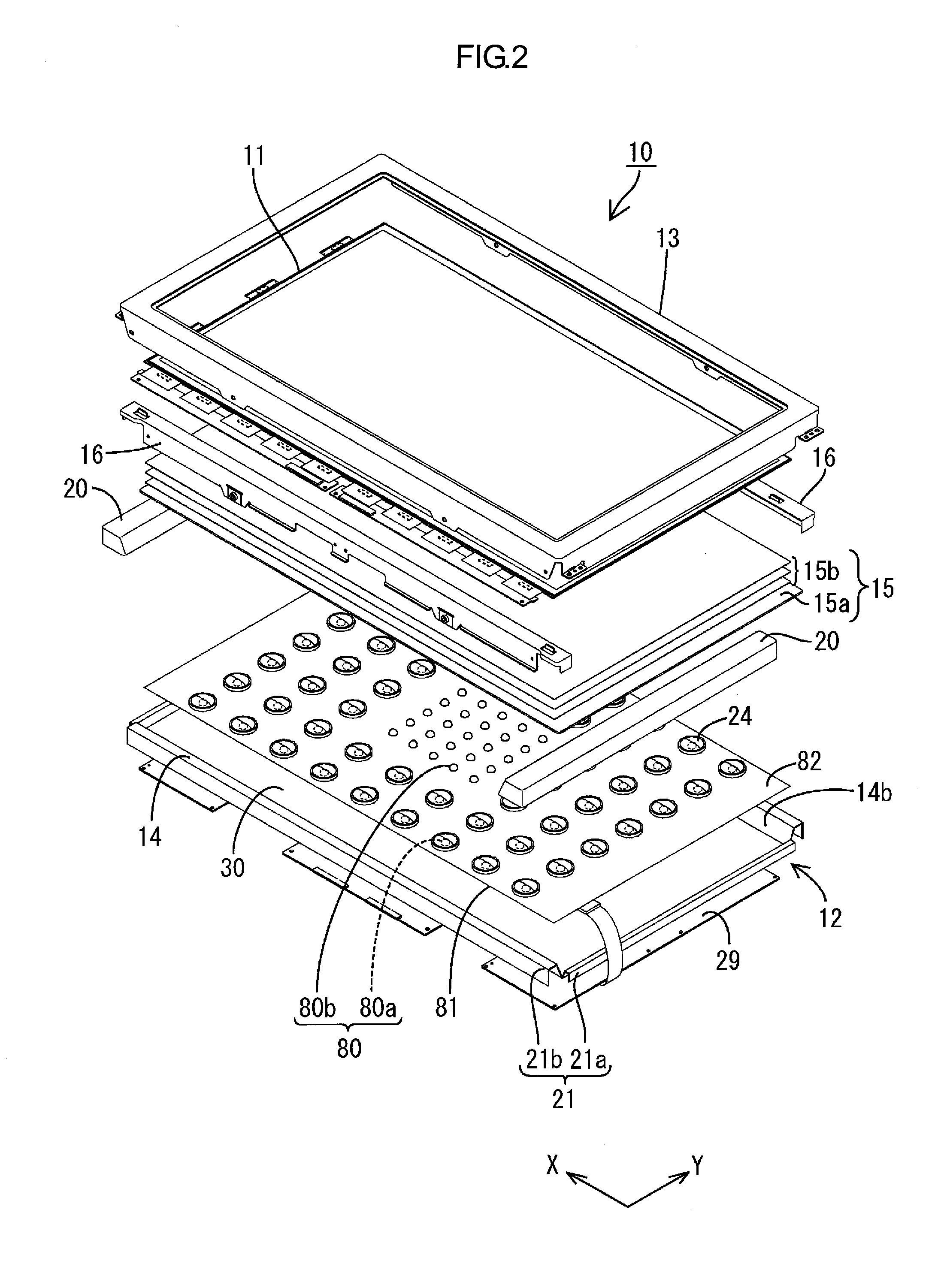
[0062]In a liquid crystal display device 10 included in a television receiver TV of the second embodiment, the diffuser lenses 24 are omitted from the backlight unit 12 of the first embodiment, and the others are the same as those of the first embodiment. The same constituent parts as those of the above first embodiment are indicated by the same symbols without repeating overlapping descriptions.

[0063]The backlight unit 12 employed for the second embodiment has the LED light sources 80 provided on the LED board 81. The LED light sources 80 are arranged on the LED board 81 such that the light source high-density area LH where the arrangement interval of the LED light sources 80 is relatively small is formed in the center area (that is, the center area of the chassis 14) of the LED board 81, and the light source low-density area LL where the arrangement interval of the LED light ...


PUM


Abstract

It is an object of the present invention to provide a lighting device realizing reduction in cost and suppression of power consumption and suppressing generation of a lamp image. A lighting device 12 of the present invention includes a plurality of point light sources 80; a chassis 14 housing the point light sources 80 and having an opening 14b through which light from the point light sources 80 exits; and an optical member 15 (15a) facing the point light sources 80 and provided to cover the opening 14b. The point light sources 80 are arranged such that a light source high-density area LH where an arrangement interval thereof is relatively small and a light source low-density area LL where an arrangement interval thereof is relatively large are provided. Light reflection portions 50 reflecting lights from the point light sources 80 are formed in at least a region overlapping with the light source low-density area LL in the optical member 15 (15a).

Description

TECHNICAL FIELD[0001]The present invention relates to a lighting device, a display device and a television receiver.BACKGROUND ART[0002]For example, a liquid crystal panel used for a liquid crystal display device such as a liquid crystal television does not emit light, and thus a backlight unit is required as a separate lighting device. The backlight unit is known, which is placed behind the liquid crystal panel (on a side opposite to a display surface side). The backlight unit includes a chassis having an opening on a liquid crystal panel side surface, numerous light sources (for example, LEDs) housed in the chassis as lamps, and an optical member (diffuser and the like) provided in the opening of the chassis and efficiently discharging light emitted from the light sources to the liquid crystal panel side.[0003]When the light sources emit point-like light in the backlight unit, the point-like light is converted into planar light by the optical member to uniform in-plane brightness ...

Claims


Application Information

Patent Timeline
IPC IPC(8): H04N3/14G02F1/13357F21V7/00
CPCG02F1/133603G02F1/133611G02F2001/133607G02F1/133605G02F2001/133613G02F1/133613G02F1/133607
Inventor YOKOTA, MASASHI
Owner SHARP KK
Why Eureka
Try Eureka