


Quick Research
Generate reliable direction feasibility study reports for your R&D in just a few steps.

Technical Q&A
Discover and master advanced knowledge NOW. Basics, ideas, possibilities, all at once.

Find Solutions
As an expert in R&D theories, this can generate solutions to your technical problems instantly.

Evaluate Feasibility
Analyze your overall solution with one click, know your potential R&D risks in advance.

Monitor Landscape
Get weekly tech updates, stay abreast of the latest tech innovations and key insights.
Integration type surface plasmon logic circuit
A surface plasmon, logic technology, applied in logic circuits, logic circuits using optoelectronic devices, logic circuits using specific components, etc. Output signal stability and other issues, to achieve the effect of reducing cost and difficulty, small size, and long transmission distance
- Summary
- Abstract
- Description
- Claims
- Application Information
AI Technical Summary
Problems solved by technology
Method used
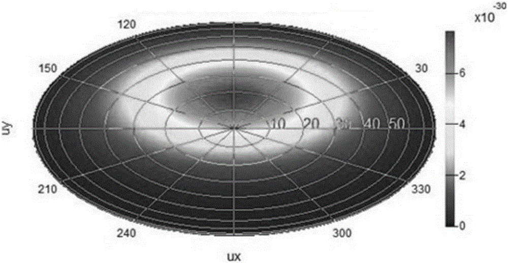
Image


Examples
Embodiment 1
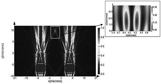
[0028] Fig. 2 shows the simulated light intensity distribution diagram of the "AND" logic gate of the present invention. The working principle is as follows: Two beams of coherent light are respectively injected from the input terminal A and input terminal C, after passing through the Fresnel zone plate, they converge at the output terminal D and perform interference calculation, and are detected by the optical power meter placed here at the same time light intensity. Since the coupling coefficient of the coupled output grating or slit is different due to the manufacturing process, for each specific device, a normalized intensity spectrum is defined. When all the components participating in the interference are in the same phase, the output intensity is the strongest, which is defined as normalized Intensity 1, defined as normalized intensity 0 when completely interfering and destructive. For the input terminal, it is defined as logic "1" when there is light injection, and log...
Embodiment 2
[0031] The working principle is the same as that of Embodiment 1. Table 1 shows the optical logic operation results of the "OR" gate. Unlike the "AND" gate, the threshold of the "OR" gate is changed. When doing "OR" logic gate operation, for the output terminal, according to the normalized intensity spectrum, the optical power greater than 0.2 is defined as logic "1", and less than 0.1 is defined as logic "0", such as image 3 As shown, this threshold is defined as "Threshold 2". According to the optical logic operation results and the definition of "threshold", Table 2 gives the corresponding truth table, which reflects the "OR" logic relationship between input terminal A and input terminal C, and realizes the function of "OR" logic gate.
Embodiment 3
[0033] The working principle is the same as that of Embodiment 1 and the definition of "threshold 2" is adopted. Table 1 shows the result of the "exclusive OR" optical logic operation and the corresponding truth table. Among them, "-I" and "I" indicate that the light intensity is the same, but the phase difference is "π". The truth table reflects the "exclusive OR" logic relationship between the input terminal A and the input terminal C, and realizes the function of the "exclusive OR" logic gate.
PUM
 Abstract
Description
Claims
Application Information
 - R&D Engineer
- R&D Manager
- IP Professional
- Industry Leading Data Capabilities
- Powerful AI technology
- Patent DNA Extraction
Browse by: Latest US Patents, China's latest patents, Technical Efficacy Thesaurus, Application Domain, Technology Topic, Popular Technical Reports.
© 2024 PatSnap. All rights reserved.Legal|Privacy policy|Modern Slavery Act Transparency Statement|Sitemap|About US| Contact US: help@patsnap.com