
Method for putting pure ultrathin two-dimensional materials on stacking top layer

A two-dimensional material and stacking technology, which is applied in the direction of electrical components, semiconductor/solid-state device manufacturing, circuits, etc., can solve the problems that PPC cannot stick to the bottom material and the bottom material is curled

Active Publication Date: 2017-02-15
INST OF METAL RESEARCH - CHINESE ACAD OF SCI
View PDF5 Cites 8 Cited by
  • Summary
  • Abstract
  • Description
  • Claims
  • Application Information

AI Technical Summary

Problems solved by technology

Once the bottom layer is larger than the top layer material, the phenomenon that the PPC glue cannot adhere to the bottom layer material, or the bottom layer material is curled

Method used


Image

  • Method for putting pure ultrathin two-dimensional materials on stacking top layer
  • Method for putting pure ultrathin two-dimensional materials on stacking top layer
  • Method for putting pure ultrathin two-dimensional materials on stacking top layer

Examples


Embodiment 1

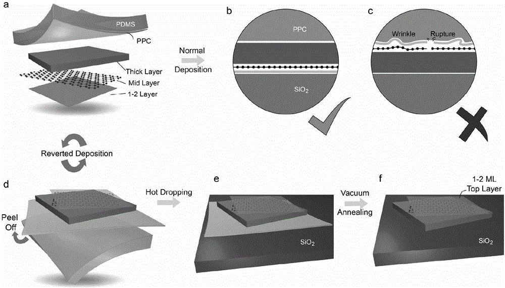
[0035] MoS with a thickness of about 5nm 2 A few layers of materials are transferred to the second layer of ultra-thin h-BN with only two atomic layers by using the first layer of h-BN with a thickness of about 15nm, and finally form a planar heterojunction with a three-layer structure and adhere to the surface of PPC superior. The PPC is coated on a solid arc-shaped PDMS prepared by the droplet method. After peeling off the 3-layer structure from PDMS, place it upside down on the surface of a clean silicon wafer, and prepare half of the MoS 2 Tunneling field effect transistor with two atomic layers of BN coverage (see Figure 7 , 1, 2, 3, 4, 9, 10 electrodes in figure a, where figure b shows the IV curve between electrodes 2-3, and figure c shows the field effect curve between electrodes 2-3), and the other half is normal MoS2 FET (see Figure 7 , 5, 6, 7, 8 electrodes in figure a, among them, figure d shows the IV curve between electrodes 6-7, and figure e shows the field...

Embodiment 2

[0037] The single-layer graphene is bonded with a layer of h-BN with a thickness of about 15nm, and finally a planar heterojunction with a 2-layer structure is formed and adhered to the surface of the PPC. The PPC is coated on a solid arc-shaped PDMS prepared by the droplet method. After the two-layer structure was peeled off from the PDMS, it was placed upside down on the surface of a clean silicon wafer, and a heterogeneous structure of ultra-pure top layer graphene on the surface of boron nitride was prepared. Since the structure maintains the flatness and purity of graphene, it can be used for scanning tunneling microscope observation and research on its electrical properties such as ultra-high mobility.


PUM

PropertyMeasurementUnit
thicknessaaaaaaaaaa
thicknessaaaaaaaaaa

Abstract

The present invention provides a method for putting pure ultrathin (the lowest layer is a monatomic layer) two-dimensional materials with high quality, ultra flatness and without glue residual on the stacking plane heterojunction top layer. The method comprises: transferring the two-dimensional materials to the surface of the viscous polymer, after repeating the step many times, and obtaining a two-dimensional heterojunction structure; and performing mechanical separation of the viscous polymer which has a surface with the heterojunction structure, putting the viscous polymer on a substrate to allow the stacking structure to perform fusion and remaining and to be an inversion state, performing the technology such as vacuum annealing and the like, completely volatilizing the polymer pressed at the bottom of the materials, and completing the purpose that the ultrathin (the lowest layer is a monatomic layer) two-dimensional materials are putted to the stacking top layer.

Description

technical field [0001] The invention belongs to the field of nano artificial composites, preparation of nanomaterial heterogeneous structures, and application research fields of micro-nano devices, sensors, etc., and specifically provides a method for placing pure ultra-thin two-dimensional materials on the top layer of stacking. Background technique [0002] Using van der Waals force to cleave layered materials to a few layers or even a single layer limit is currently the main method to obtain the highest quality two-dimensional materials. In the two-dimensional limit, materials usually exhibit properties that many bulk materials do not have, such as the quantum Hall effect. The heterostructure in which different two-dimensional materials are coupled together through the interface of artificial methods has become an international research hotspot in recent years. The heterojunction of two-dimensional materials includes interface coupling between two-dimensional materials, ...

Claims


Application Information

Patent Timeline
Patent Type & Authority Applications(China)
IPC IPC(8): H01L21/34H01L21/28H01L29/739
CPCH01L21/28H01L29/66969H01L29/7391
Inventor 韩拯张志东李小茜刘卫来陈茂林
Owner INST OF METAL RESEARCH - CHINESE ACAD OF SCI
Learn More