Display device, display panel and manufacturing method thereof

A technology for display panels and array substrates, which is applied in the fields of instruments, nonlinear optics, optics, etc., can solve the problems of increasing the cost of color filter substrates and the influence of the preparation process, and achieve the effect of reducing the complexity of the preparation process.

Active Publication Date: 2019-09-03
SHANGHAI AVIC OPTOELECTRONICS +1
View PDF5 Cites 0 Cited by
  • Summary
  • Abstract
  • Description
  • Claims
  • Application Information

AI Technical Summary

Problems solved by technology

[0004] exist figure 1 In the liquid crystal display panel shown, since one side of the color filter substrate needs to make a touch electrode layer, and the other side needs to make a black matrix layer and a color resist layer, the preparation processes of the film layers on both sides may affect each other , and because most of the color filter substrates are outsourced, using the double-sided manufacturing process to make the color filter substrate will increase the cost of outsourcing the color filter substrate

Method used


Image

  • Display device, display panel and manufacturing method thereof
  • Display device, display panel and manufacturing method thereof
  • Display device, display panel and manufacturing method thereof

Examples


Embodiment Construction

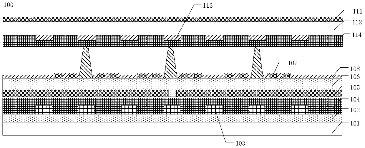
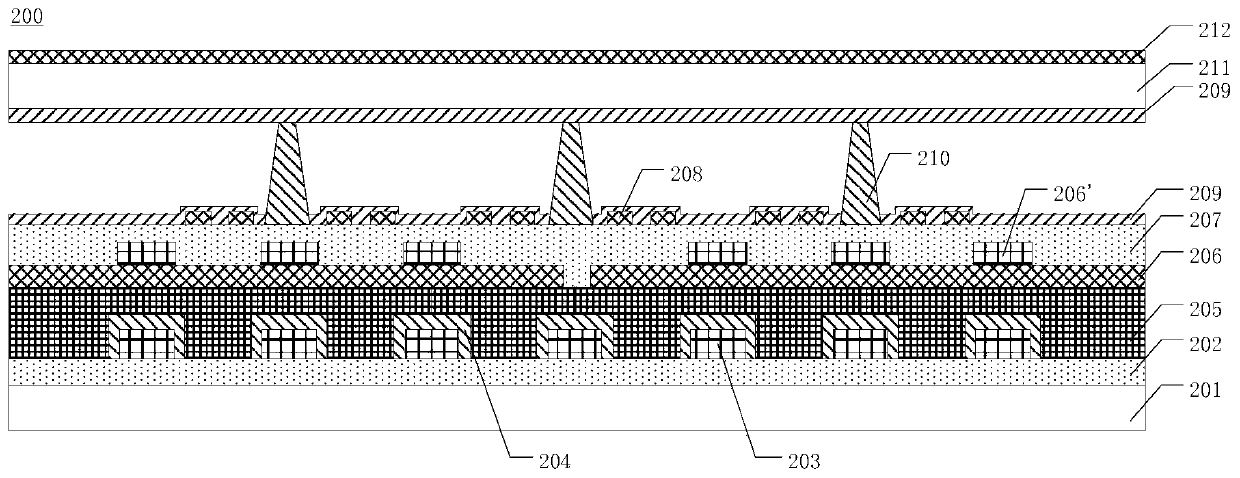
[0031] Example embodiments will now be described more fully with reference to the accompanying drawings. However, the example embodiments can be implemented in various forms, and should not be construed as being limited to the examples set forth herein; on the contrary, the provision of these embodiments makes the present disclosure more comprehensive and complete, and fully conveys the concept of the example embodiments To those skilled in the art. The described features, structures or characteristics can be combined in one or more embodiments in any suitable way. In the following description, many specific details are provided to give a sufficient understanding of the embodiments of the present disclosure. However, those skilled in the art will realize that the technical solutions of the present disclosure can be practiced without one or more of the specific details, or other methods, components, devices, steps, etc. can be used. In other cases, the known technical solution...


PUM

PropertyMeasurementUnit
thicknessaaaaaaaaaa

Abstract

The invention provides a display device, a display panel and a preparation method of the display panel. The display panel comprises an array substrate, an opposite substrate opposite to the array substrate, a color resistance layer, a plurality of first touch electrodes and a plurality of second touch electrodes, wherein the array substrate comprises a plurality of sub-pixel regions, and each sub-pixel region comprises one or more TFTs (thin film transistors); the color resistance layer is arranged on the array substrate, is located between the array substrate and the opposite substrate and comprises a plurality of color resistance blocks, and each color resistance block is correspondingly located in one sub-pixel region; the plurality of first touch electrodes are arranged on the array substrate and located between the array substrate and the opposite substrate; the plurality of second touch electrodes are arranged on the side, deviated from the array substrate, of the opposite substrate. The preparation cost of the display panel provided by the invention can be reduced.

Description

Technical field [0001] The present disclosure relates to the field of display technology, and in particular, to a display panel, a preparation method of the display panel, and a display device including the display panel. Background technique [0002] With the development of optical technology and semiconductor technology, liquid crystal display (LCD) has the characteristics of lighter and thinner, lower cost and energy consumption, faster response speed, better color purity and brightness, and higher contrast. It has been widely used in various electronic products. [0003] At the same time, with the popularization of touch interaction methods, more and more flat panel display devices begin to integrate touch modules. For example, figure 1 A liquid crystal display panel integrated with a touch module is shown in the figure, which mainly includes: an array substrate 101 formed with a TFT (Thin Film Transistor) array, a first insulating layer 102 on the array substrate 101, and dat...

Claims


Application Information

Patent Timeline
Patent Type & Authority Patents(China)
IPC IPC(8): G02F1/1333G02F1/1335G02F1/1343G02F1/1362
CPCG02F1/1333G02F1/13338G02F1/133514G02F1/134309G02F1/136209G02F1/136222
Inventor 秦丹丹曹兆铿
Owner SHANGHAI AVIC OPTOELECTRONICS
Why Eureka
Try Eureka