
Wafer-level package mems chip with vertical pads and manufacturing method thereof

A wafer-level packaging and manufacturing method technology, applied in the field of MEMS chips, can solve the problems of high cost and complicated process, and achieve the effect of convenient subsequent packaging and simple operation process

Active Publication Date: 2017-08-04
ANHUI BEIFANG XINDONG LIANKE MICROSYST TECH
View PDF5 Cites 0 Cited by
  • Summary
  • Abstract
  • Description
  • Claims
  • Application Information

AI Technical Summary

Problems solved by technology

In the prior art, the production of vertical bonding pads is carried out in the packaging stage after the main production process of the main chip is completed, or the carrier board that only serves to connect electrical signals is produced separately. These methods require additional production processes to form Vertically press the welding block, the process is complicated and the cost is high

Method used


Image

  • Wafer-level package mems chip with vertical pads and manufacturing method thereof
  • Wafer-level package mems chip with vertical pads and manufacturing method thereof
  • Wafer-level package mems chip with vertical pads and manufacturing method thereof

Examples


Embodiment 1

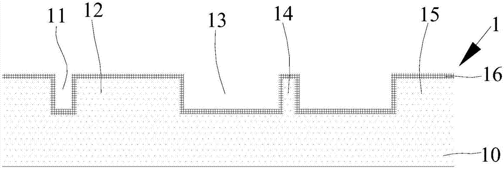
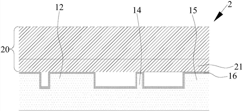
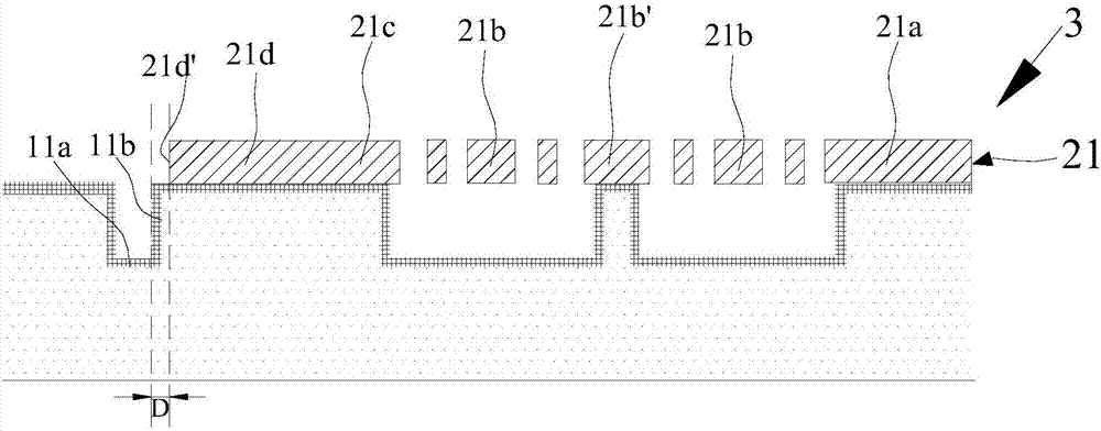
[0031] A method for manufacturing a wafer-level package MEMS chip with a vertical pressure welding block, comprising the following steps:

[0032](1) Fabrication of base plate wafer 1: use double-sided polished single-crystal Si wafer 10 as the base plate material, and after photolithography process steps such as coating photoresist, alignment, exposure, and development (hereinafter referred to as photolithography), A photoresist pattern is formed on the double-sided polished single-crystal Si wafer 10, and the photoresist pattern is used as a mask for deep Si reactive ion etching (DRIE), and Si is etched in a reaction atmosphere containing fluorine (F), and the reaction The gas used is usually SF 6 and C 4 f 8 , where SF 6 is the isotropic etching gas, C 4 f 8 is the gas that produces polymers, alternating SF in reactive ion etching equipment 6 and C 4 f 8 , etch a 50-200 μm deep pattern on a double-sided polished single-crystal Si wafer 10, remove the photoresist, an...

Embodiment 2

[0045] The fabrication method of the wafer-level package MEMS chip 7 with vertical pads in this embodiment is similar to the fabrication method of Embodiment 1, the only difference is that step (1) also makes chamfers 11c on the top of the bottom groove 11, An insulating layer 16 is also grown on the chamfer 11c; step (4) also deposits a metal layer 34 on the insulating layer 16 on the slope of the chamfer 11c, and due to the existence of the chamfer 11c, it is also beneficial to the metal layer 34 in step (4). 34 evenly covers the chamfer 11c slope and the bottom plate groove side 11b.

[0046] The difference between the wafer-level package MEMS chip 7 with vertical pads produced in this embodiment and the wafer-level package MEMS chip 7 with vertical pads produced in Embodiment 1 is only that the top of the groove 11 on the bottom plate has a chamfer 11c, the metal layer 34 is also deposited on the slope of the chamfer 11c, such as Figure 12 shown.


PUM

PropertyMeasurementUnit
Depthaaaaaaaaaa
Thicknessaaaaaaaaaa
Thicknessaaaaaaaaaa

Abstract

The invention discloses a wafer-level package MEMS chip with vertical pressure welding block and a method for manufacturing the same. The wafer-level package MEMS chip comprises a cover plate, an MEMS structure layer and a bottom plate, the upper surface of the bottom plate has a bottom plate groove, and the surface and the side surface of the bottom plate groove have an insulating layer. The metal layer is deposited on the upper surface and the end face of the MEMS lead area and the insulating layer of the bottom plate groove, the metal layer is in electrical contact with the MEMS lead area, the metal layer located in the MEMS lead area is used as a horizontal pressure welding block, and the metal layer on the insulating layer of the bottom plate groove is the vertical pressure welding block. Under the premise of not making additional process, the vertical pressure welding block is formed as soon as the completion of the MEMS chip, so that the method for manufacturing the wafer-level package MEMS chip has the advantages of short development time, simple test and low cost, and is particularly suitable for manufacturing high-performance industrial-grade MEMS chip.

Description

technical field [0001] The invention belongs to the field of MEMS chips, and in particular relates to a wafer-level packaging MEMS chip with vertical pressure welding blocks. The invention also relates to the wafer-level packaging MEMS chip with vertical pressure welding blocks and a manufacturing method thereof. Background technique [0002] MEMS (Micro-Electro-Mechanical Systems) chips, especially MEMS inertial sensor chips, have a corresponding relationship between the sensing direction and the MEMS structure. For example, the X-axis MEMS measurement unit can only sense the inertial signal in the X-axis direction, and the Y-axis and Z-axis The axis is the same; in consumer-grade MEMS inertial sensors, the measurement units of the X, Y, and Z axes are integrated on the same MEMS chip to reduce the chip size; but in high-performance industrial-grade MEMS inertial sensors , in order to ensure the performance of the product, usually a measurement unit for one axis is made on ...

Claims


Application Information

Patent Timeline
IPC IPC(8): B81B7/00B81C3/00
CPCB81B7/007B81C3/001
Inventor 华亚平
Owner ANHUI BEIFANG XINDONG LIANKE MICROSYST TECH
Learn More