


Quick Research
Generate reliable direction feasibility study reports for your R&D in just a few steps.

Technical Q&A
Discover and master advanced knowledge NOW. Basics, ideas, possibilities, all at once.

Find Solutions
As an expert in R&D theories, this can generate solutions to your technical problems instantly.

Evaluate Feasibility
Analyze your overall solution with one click, know your potential R&D risks in advance.

Monitor Landscape
Get weekly tech updates, stay abreast of the latest tech innovations and key insights.
Method for manufacturing semiconductor device and substrate processing apparatus
A technology of substrate processing device and manufacturing method, which is applied in semiconductor/solid-state device manufacturing, semiconductor devices, electric solid-state devices, etc., can solve problems such as adverse effects of film characteristics, and achieve the effect of improving processing uniformity
- Summary
- Abstract
- Description
- Claims
- Application Information
AI Technical Summary
Problems solved by technology
Method used
Image


Examples
no. 1 approach
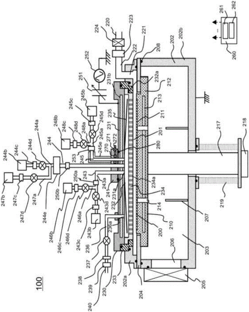
[0035] (1) Configuration of the substrate processing device
[0036] use figure 1 , figure 2 and image 3 A first embodiment of the substrate processing apparatus of the present invention will be described. It should be noted that, if figure 1 As shown, the present embodiment is an apparatus for forming a thin film on a substrate, and is configured as a single-piece substrate processing apparatus that processes one substrate at a time.
[0037] (processing room)
[0038] Such as figure 1 As shown, the substrate processing apparatus 100 includes a processing vessel 202 . The processing container 202 is configured, for example, as a closed container having a circular cross section and a flat shape. In addition, the side wall and the bottom wall of the processing container 202 are made of metal materials such as aluminum (Al) and stainless steel (SUS), for example. A processing chamber 201 for processing a wafer 200 such as a silicon wafer as a substrate and a transfer s...
Deformed example 1
[0219] Next, use Figure 7 and Figure 8 Modification 1 of the present invention will be described. The substrate processing apparatus of Modification 1 differs from the substrate processing apparatus of the first embodiment only in that Figure 7 The third gas supply system shown and the controller for controlling the third gas supply system are the same as those of the first embodiment in other configurations.
[0220] Specifically, as Figure 7As shown, in the third gas supply system 245, the following configuration is formed: between the third gas supply source 245b and the MFC 245c, a valve 245f as an on-off valve, a box 245g as a gas storage part for storing gas, and and a valve 245h as an on-off valve.
[0221] use Figure 8 The operation of the third gas supply system in Modification 1 will be described. As mentioned above, Figure 8 with the first embodiment Figure 6 The difference lies in the flow rate of the heated purge gas and the flow mode of the heated ...
Deformed example 2
[0233] Next, use Figure 9 and Figure 10 Modification 2 of the present invention will be described. The substrate processing apparatus of Modification 2 differs from the substrate processing apparatus of the first embodiment only in that Figure 9 The third gas supply system shown and the controller for controlling the third gas supply system are the same as those of the first embodiment in other configurations.
[0234] Such as Figure 9 As shown, in the third gas supply system of Modification 2, the first gas storage system and the second gas storage system are connected in parallel between the third gas supply source 245b and the MFC 245c in the third gas supply system 245 of the first embodiment. System made. The first gas storage system is configured to include a valve 245f as an on-off valve, a tank 245g as a gas storage portion for storing gas, and a valve 245h as an on-off valve. The second gas storage system is configured in the following manner: it is provided ...
PUM
 Abstract
Description
Claims
Application Information
 - R&D Engineer
- R&D Manager
- IP Professional
- Industry Leading Data Capabilities
- Powerful AI technology
- Patent DNA Extraction
Browse by: Latest US Patents, China's latest patents, Technical Efficacy Thesaurus, Application Domain, Technology Topic, Popular Technical Reports.
© 2024 PatSnap. All rights reserved.Legal|Privacy policy|Modern Slavery Act Transparency Statement|Sitemap|About US| Contact US: help@patsnap.com