An alignment system and alignment method for automatic focusing

An automatic focusing and aligning system technology, applied in the photoengraving process, instruments, optics and other directions of the pattern surface, can solve the problems of complex structure, difficult realization, difficult and clear imaging of alignment marks, etc., to achieve rapid focusing, The effect of reducing the impact

Active Publication Date: 2019-01-29
SHANGHAI MICRO ELECTRONICS EQUIP (GRP) CO LTD
View PDF6 Cites 0 Cited by
  • Summary
  • Abstract
  • Description
  • Claims
  • Application Information

AI Technical Summary

Problems solved by technology

[0005] This technology solves the problems of complex structure, high installation and adjustment difficulty and difficult implementation when using a self-referencing interferometer to determine the position of the alignment mark
However, before the detector unit obtains the horizontal relative position relationship between the alignment mark and the reference mark, it must first obtain a clear image of the alignment mark. Due to environmental interference and increasingly small chip size, the alignment mark on the silicon wafer is very difficult It is difficult to image clearly, so it is necessary to invent an optical path alignment system that can solve the problem that the alignment system is easily disturbed by the environment and it is difficult to search for the best focal plane for small-sized alignment marks on silicon wafers

Method used


Image

  • An alignment system and alignment method for automatic focusing
  • An alignment system and alignment method for automatic focusing
  • An alignment system and alignment method for automatic focusing

Examples


Embodiment 1

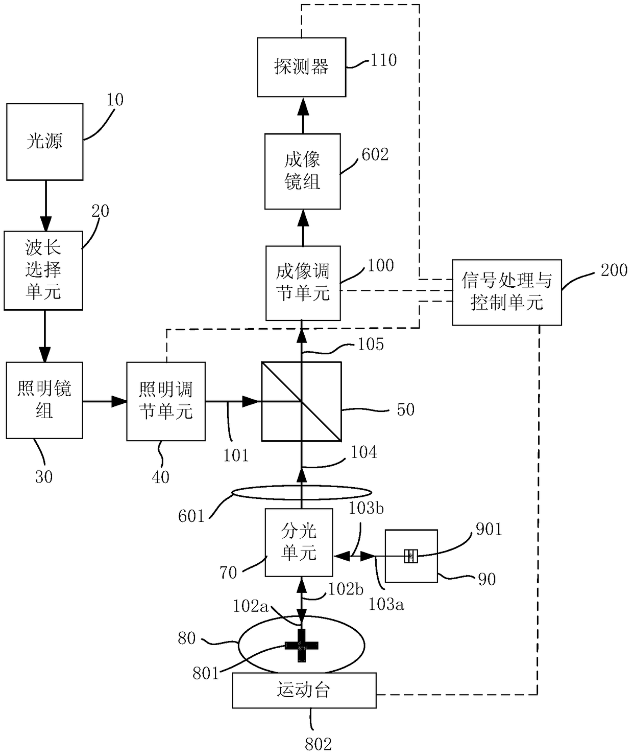
[0043] figure 1 It is a schematic structural diagram of the automatic focusing alignment system provided by the present invention, as shown in the figure, the automatic focusing system at least includes:

[0044] The light source 10 is used to provide an illumination light source;

[0045] A wavelength selection unit 20, configured to filter optical signals with interfering wavelengths or bandwidths;

[0046] The illuminating mirror group 30 is used to provide illuminating light for the alignment marks 801 on the surface of the silicon wafer 80;

[0047] An illumination adjustment unit 40, configured to switch between a manual illumination mode and an automatic illumination mode and adjust light intensity and polarization state distribution, etc. for the marks on the surface of the silicon wafer 80;

[0048] The beam splitting unit 50 is used for vertically distributing and splitting the passing illumination light path and the passing reflection light path;

[0049] The refer...

Embodiment 2

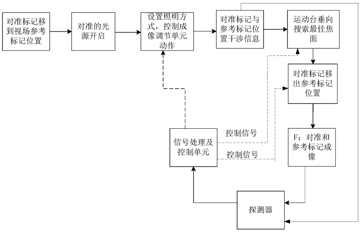
[0074] Such as Figure 10 As shown, the difference between this embodiment and Embodiment 1 is that the measurement reflected light path 102b is taken as the axis, the first reflected light path 104 and the second reflected light path 105 are coaxial with the measured reflected light path 102b, and the The angle formed by the measurement incident light path 102a and the axis where the measurement reflection light path 102b is located is between 0° and 90°, and this off-axis lighting method can improve contrast and reduce interference. In addition, a shutter 902 is installed on the optical path of the reference mark 901 for switching. After the photolithography of the first silicon wafer, the shutter 902 can be used to close the reference incident light path 103a incident on the reference mark 901. The alignment system can automatically search for the best focal plane position z according to the alignment data records of the first silicon wafer, and at the same time, it can avo...

Embodiment 3

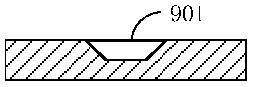
[0076] Such as Figure 11 As shown, the difference between this embodiment and Embodiment 1 and Embodiment 2 is that the cross-section of the reference mark 901 is an isosceles trapezoid that is convex relative to the reference mark surface 90 .


PUM


Abstract

The invention provides an aligning system for an automatic focusing and an aligning method. The aligning system comprises a light source, a wavelength selection unit, an illumination mirror set, an illumination adjusting unit, a beam splitting unit, an imaging objective lens set, a splitting unit, a reference mark face and a reference mark, a silicon wafer and an aligning mark, and a motion bench in sequence. The splitting unit is connected to the imaging regulating unit, an imaging mirror set, and a detector in sequence, and the detector, the imaging regulating unit, the illumination adjusting unit, and the motion bench are connected to a signal processing and controlling unit. A beam of illumination light illuminates the reference mark and the aligning mark at the same time. The system searches and marks an optimal focal plane of the reference mark, and calculates the interference envelope extremum formed by the interferometric fringe of light reflected by the reference mark and the aligning mark in an area of the reference mark, and the deviation value of the aligning mark and the optimal focal plane can be determined. The aligning mark is moved to the optimal focal plane to complete focusing. The system can automatically, accurately, and fast focus, and reduce the effect that the precision is affected by the environment.

Description

technical field [0001] The invention relates to the field of semiconductor photolithography, in particular to an automatic focusing alignment system and alignment method. Background technique [0002] In the manufacturing process of semiconductor IC integrated circuits, a complete chip usually needs to undergo multiple photolithography exposures before it can be completed. Except for the first photolithography, the photolithography of other levels must be accurately positioned before exposure, so as to ensure the correct relative position between the graphics of each layer. Instant overlay accuracy. Normally, the overlay accuracy is 1 / 3 to 1 / 5 of the resolution index of the lithography machine. For a 100nm lithography machine, the overlay accuracy index is required to be less than 35nm. When the feature size CD is required to be smaller, the requirements for overlay accuracy and the resulting alignment accuracy become more stringent. For example, a 90nm CD size requires an...

Claims


Application Information

Patent Timeline
Patent Type & Authority Patents(China)
IPC IPC(8): G03F7/207G03F9/02
Inventor 于大维
Owner SHANGHAI MICRO ELECTRONICS EQUIP (GRP) CO LTD
Why Eureka
Try Eureka