
Cooling structure of package chip

A heat dissipation structure and chip technology, applied in the direction of electrical components, electric solid devices, circuits, etc., can solve the problems of distance error, affecting chip performance and service life, slow emission, etc., and achieve the effect of overcoming installation errors and improving EMC performance

Active Publication Date: 2016-12-07
四川苏格通讯技术有限公司 +1
View PDF8 Cites 8 Cited by
  • Summary
  • Abstract
  • Description
  • Claims
  • Application Information

AI Technical Summary

Problems solved by technology

[0004] Due to some errors in the distance between the shield and the chip, when the error is large, the thermal paste often cannot touch the shield, which makes the temperature in the shield dissipate slowly under the limitation of hot poor conductor air, making The chip is in a high temperature state for a long time, which greatly affects the performance and service life of the chip

Method used


Image

  • Cooling structure of package chip
  • Cooling structure of package chip
  • Cooling structure of package chip

Examples


Embodiment Construction

[0027] The present application will be further elaborated below in conjunction with specific embodiments. It should be understood that these examples are only used to illustrate the present application and are not intended to limit the scope of the present application.

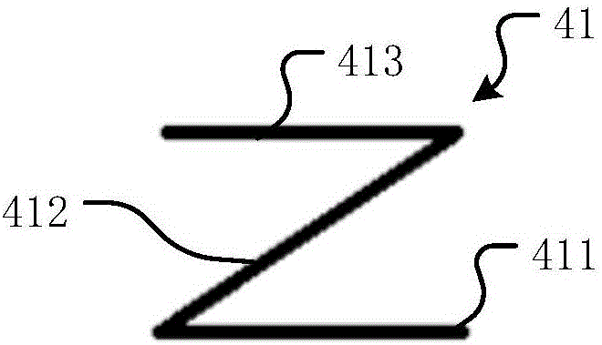
[0028] Such as figure 2 As shown, the heat dissipation structure 100 for packaged chips in one embodiment of the present application generally includes a PCB board 10, a chip 20 mounted on the PCB board 10, a shielding case 30 packaged on the PCB board 10 and covering the chip 20, And the heat sink 40 is arranged between the upper surface of the chip 20 and the lower surface of the shielding case 30 and has an elastic movable range.

[0029] Through the elastic heat sink 40, the height error between the chip 20 and the shield 30 can be completely overcome, so that the heat can be transmitted to the shield 30 through the heat sink 40 as soon as possible, and then dissipated by the external heat dissipation co...


PUM


Abstract

The invention relates to the field of chip package, in particular to a cooling structure of a package chip. The cooling structure comprises a printed circuit board (PCB), a chip, a shielding cover and a heat sink, wherein the chip is arranged on the PCB, the shielding cover is packaged on the PCG and covers the chip, and the heat sink is arranged between an upper surface of the chip and a lower surface of the shielding cover and has an elastic activity range. In the cooling structure, an elastic metal element is used as the heat sink, an installation error between the chip and the shielding cover can be overcome, the chip heat is rapidly dissipated out, the problems that an electronic product is large in heat generation and slow in heat dissipation and the application performance is reduced, the service lifetime is shortened and the reliability is poor when the chip is in a high-temperature working condition for a long time are solved, and meanwhile, the electromagnetic compatibility (EMC) performance of the chip can also be improved.

Description

technical field [0001] The present application relates to the field of chip packaging, and specifically relates to a heat dissipation structure capable of overcoming errors in the installation of packaged chips and quickly dissipating heat from the chips. Background technique [0002] A chip (Chip) in the prior art generally refers to a carrier of an integrated circuit, and is also a result of the design, manufacture, packaging, and testing of the integrated circuit, and is usually an independent whole that can be used immediately. Integrated circuits that handle high power require thermal management for reliability reasons, so all chips have a safe upper limit on junction temperature, usually 150°C (sometimes 175°C). The cooler the operating temperature, the longer the life of the chip. [0003] Such as figure 1 As shown, when the chip is packaged on the PCB, its outer surface is also covered with a shield, and the bottom surface of the packaged shield is still a certain ...

Claims


Application Information

Patent Timeline
Patent Type & Authority Applications(China)
IPC IPC(8): H01L23/367
CPCH01L23/367
Inventor 夏俊稳曾永聪
Owner 四川苏格通讯技术有限公司
Learn More