A wave soldering carrier

A wave soldering and carrier technology, applied in welding equipment, manufacturing tools, metal processing, etc., can solve problems such as the inability to meet high-precision component floating requirements, the impact on production efficiency, and the impact on efficiency, and is conducive to automation, reducing Wasteful, easy-to-use effects

Active Publication Date: 2019-05-24
WEIFANG GOERTEK ELECTRONICS CO LTD
View PDF9 Cites 0 Cited by
  • Summary
  • Abstract
  • Description
  • Claims
  • Application Information

AI Technical Summary

Problems solved by technology

The original pressure plate pressing floating height mode cannot meet the floating height requirements of such high-precision components due to the tolerance of the flatness of the pressure plate processing and the tolerance of the body size when the components are manufactured.
In addition, the pressure plate and the carrier need to be operated separately, and manual positioning and placement are required during use, which has a certain impact on production efficiency.
In addition, when the gravity of the pressure plate cannot overcome the buoyancy of the components, it is necessary to add an additional pressure supply device to provide pressure for the pressure plate, and redundant actions will occur, which will have a greater impact on efficiency

Method used


Image

  • A wave soldering carrier
  • A wave soldering carrier

Examples


Embodiment Construction

[0021] In order to make the object, technical solution and advantages of the present invention clearer, the implementation manner of the present invention will be further described in detail below in conjunction with the accompanying drawings.

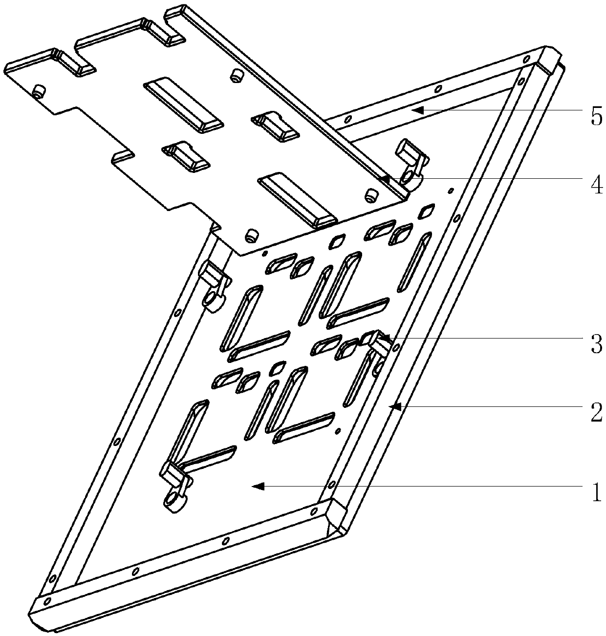
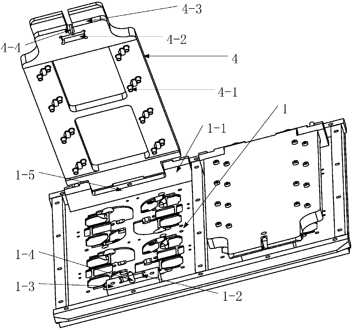
[0022] figure 2 A wave soldering carrier provided for one embodiment of the present invention. Such as figure 2 As shown, a wave soldering carrier includes a bottom plate 1, a pressure plate 4 is arranged on the bottom plate 1, a support block 1-1 is arranged on the bottom plate 1, one end of the pressure plate 4 is hinged with the support block 1-1, and the support block 1-1 limits The pressure plate 4 rotates around the hinge axis within the preset angle range, and when the pressure plate 4 rotates to the open state, the support block 1-1 limits and fixes the pressure plate 4; the side of the pressure plate 4 facing the bottom plate 1 is provided with a corresponding circuit board The spring probe 4-1 of the upper component, when...


PUM


Abstract

The invention discloses a wave-soldering carrier which comprises a bottom plate, wherein a pressing plate and a back-up block are arranged on the bottom plate; one end of the pressing plate is hinged to the back-up block; the back-up block limits the pressing plate to rotate around a hinge shaft within a preset angle range, and when the pressing plate rotates to the open state, the back-up block fixes the pressing plate in a limiting manner; one or more spring probes corresponding to a component on a circuit board is / are arranged on the side, facing the bottom plate, of the pressing plate; when the pressing plate and the bottom plate are buckled, the spring probe(s) press / presses the component on the circuit board, so that the lower surface of the component is in close fit with the upper surface of the circuit board. According to the invention, the spring probe(s) is / are arranged on the pressing plate, so that the component and the circuit board are in close contact to meet the zero floating height requirement; the pressing plate and the wave-soldering carrier realize integration through hinge joint, so that inconvenience during production circulation is overcome, and waste caused by turnover of human resources is reduced; the adopted hinge joint operation is convenient and fast, and the opening position of the pressing plate is fixed in a limiting manner to facilitate automation of the production flow.

Description

technical field [0001] The invention relates to the technical field of wave soldering, in particular to a wave soldering carrier. Background technique [0002] Such as figure 1 As shown, it is a wave soldering carrier in the prior art. The bottom plate 1 is mainly used to carry PCBA (Printed Circuit Board Assembly, printed circuit board assembly), and there are through holes for wave soldering and components protection on it. Sink, and positioning pins to ensure that the PCBA is placed in the correct position every time; the side strip 2 is used to prevent high-temperature liquid tin from entering the upper surface of the tooling and contacting the PCBA; the buckle 3 can be rotated and buckled on the PCBA to fix the PCBA On the bottom plate, and provide pressure to make the PCBA overcome the buoyancy and impact force it bears during welding; the main function of the pressure plate 4 is to use gravity or additional external pressure to press down the easy-to-float components...

Claims


Application Information

Patent Timeline
Patent Type & Authority Patents(China)
IPC IPC(8): B23K3/00B23K3/08H05K3/34B23K101/42
CPCB23K3/00B23K3/087H05K3/34
Inventor 朱军文
Owner WEIFANG GOERTEK ELECTRONICS CO LTD
Why Eureka
Try Eureka