
A processing fixture and processing method for realizing aluminum-nickel bonding of ceramic chip packaging devices

A patch packaging and processing method technology, which is applied in the manufacture of semiconductor devices, electric solid devices, semiconductor/solid devices, etc., can solve problems such as inability to achieve quantitative uniformity, affect device quality, and affect bonding strength. Clamping and alignment time, ensuring appearance quality, and avoiding assembly difficulties

Active Publication Date: 2019-05-14
CHINA ZHENHUA GRP YONGGUANG ELECTRONICS CO LTD STATE OWNED NO 873 FACTORY
View PDF5 Cites 0 Cited by
  • Summary
  • Abstract
  • Description
  • Claims
  • Application Information

AI Technical Summary

Problems solved by technology

[0002] For a long time, in the manufacturing process of semiconductor power devices, aluminum wires are directly bonded to gold-plated parts, and aluminum wires are directly bonded to the surface of gold-plated dies. In theory, there will be Kirkendall voids in the bonding between gold and aluminum. Kendall voids will affect the bonding strength and may lead to debonding, seriously affecting the quality of the device
Moreover, during the assembly process of nickel-plated copper sheets, it is necessary to install positioning sleeves in the cavity on the tube base one by one. After installing the positioning sleeves, it is necessary to quantitatively spot solder paste on the two welding areas of each tube base, and then place the nickel-plated Copper sheet, due to the small size of the transitional nickel-plated copper sheet (1.8mmX1.8m square sheet), it is difficult to place it in alignment, and the above steps are all manual operations, so the workload is large and the efficiency is low
And using manual spot solder paste, can not achieve quantitative uniformity, which has a certain impact on the sintering quality

Method used


Image

  • A processing fixture and processing method for realizing aluminum-nickel bonding of ceramic chip packaging devices
  • A processing fixture and processing method for realizing aluminum-nickel bonding of ceramic chip packaging devices
  • A processing fixture and processing method for realizing aluminum-nickel bonding of ceramic chip packaging devices

Examples


Embodiment Construction

[0028] The technical solution of the present invention is further described below, but the scope of protection is not limited to the description.

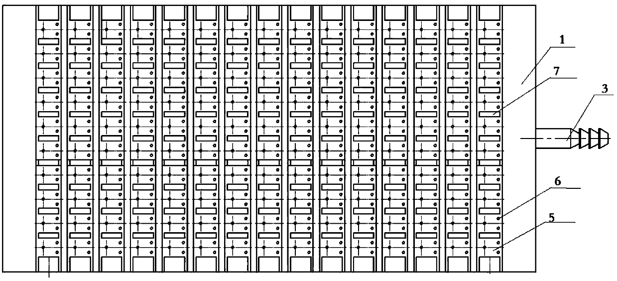
[0029] A processing fixture for realizing aluminum-nickel bonding of ceramic chip packaged devices; including a base plate 4, the base plate 4 is provided with a large-area groove in the middle of the upper end, and an air nozzle 3 is installed on one side of the base plate 4, and the air nozzle 3 is connected to the In the groove on the bottom plate 4, a rubber pad 2 is installed on the upper end of the bottom plate 4, and a plurality of cavities 5 are arranged on the upper end of the positioning plate 1, and each cavity 5 is separated by a partition 7, and the cavities There are three air holes 6 through which the positioning plate 1 is penetrated in the vertical direction.

[0030] The shape, size and area of ​​the end faces of the positioning plate 1, the rubber pad 2 and the bottom plate 4 are all the same.

[0031] The rubbe...


PUM


Abstract

The present invention provides a processing fixture for realizing aluminum-nickel bonding of a ceramic patch packaged device and a processing method therefor. The processing fixture includes a base board. A large area of groove is disposed in the middle of an upper end of the base board. A gas nozzle is mounted on one side surface of the base board. The gas nozzle is connected into the groove in the base board. A rubber pad is mounted on the upper end of the base board. Multiple cavities are disposed on an upper end of a location board. Every two adjacent cavities are separated by a clapboard. The cavity is internally provided with three air holes penetrating the location board in a vertical direction. Through adoption of the processing fixture and the processing method, debonding caused by bonding strength of gold and aluminum is prevented, and due to use of pure nickel sheets, nickel-plated copper sheets are simple to assemble, and the production efficiency is improved.

Description

technical field [0001] The invention relates to the field of semiconductor element processing, in particular to the field of processing ceramic chip packaging devices. Background technique [0002] For a long time, in the manufacturing process of semiconductor power devices, aluminum wires are directly bonded to gold-plated parts, and aluminum wires are directly bonded to the surface of gold-plated dies. In theory, there will be Kirkendall voids in the bond between gold and aluminum. Kendall voids will affect the bonding strength, may lead to debonding, and seriously affect the quality of the device. Moreover, during the assembly process of nickel-plated copper sheets, it is necessary to install positioning sleeves in the cavity on the tube base one by one. After installing the positioning sleeves, it is necessary to quantitatively spot solder paste on the two welding areas of each tube base, and then place the nickel-plated copper For the copper sheet, due to the small siz...

Claims


Application Information

Patent Timeline
Patent Type & Authority Patents(China)
IPC IPC(8): H01L21/683H01L21/60
CPCH01L21/6838H01L24/85H01L2224/85012
Inventor 唐勇丁小宏杨正义
Owner CHINA ZHENHUA GRP YONGGUANG ELECTRONICS CO LTD STATE OWNED NO 873 FACTORY
Learn More