
Circuit substrate manufacturing method and circuit substrate

A technology of circuit substrate and manufacturing method, which is applied in the direction of removing conductive materials by chemical/electrolytic methods, which can solve problems such as reduced heat release, inability to install electronic components, poor thermal conductivity of resist ink or protective layer, etc., to achieve inhibition Effects of covering and suppressing position shift

Inactive Publication Date: 2016-10-19
TOYO ALUMINIUM KK
View PDF7 Cites 0 Cited by
  • Summary
  • Abstract
  • Description
  • Claims
  • Application Information

AI Technical Summary

Problems solved by technology

In the case of a positional shift, such as Figure 29 and Figure 30 As shown, the circuit pattern metal foil 102 that must be coated with resist ink or the like will be exposed, and the component mounting portion that cannot be coated with resist ink or the like will be covered, and there is a problem that electronic components cannot be mounted.
[0008] If the component mounting part is covered with resist ink, etc., it will not be conductive even if electronic components are mounted, so the function as a circuit board cannot be realized
Therefore, the above-mentioned problems are serious problems for circuit boards.
[0009] In addition, in circuit boards for mounting heat-generating components such as LED elements, high heat dissipation is required, but the resist ink or protective layer used to cover the circuit pattern has poor heat conduction. There is a problem that heat dissipation decreases when the circuit board is covered with

Method used


Image

  • Circuit substrate manufacturing method and circuit substrate
  • Circuit substrate manufacturing method and circuit substrate
  • Circuit substrate manufacturing method and circuit substrate

Examples


Embodiment 1

[0136] 100 parts by mass of an adhesive (manufactured by DIC Corporation: trade name LX500) and 10 parts by mass of a curing agent (manufactured by DIC Corporation: trade name KW75) were mixed to prepare an adhesive resin. The adhesive resin prepared above was coated on one side of an aluminum foil (manufactured by Toyo Aluminum Co., Ltd.) with a thickness of 50 μm so that the thickness after the solvent evaporated was 3 μm, thereby forming an adhesive resin layer. A polyethylene terephthalate film (manufactured by Teijin DuPont Films Co., Ltd.) with a thickness of 38 μm was bonded on the adhesive resin layer as an insulating base material, and the insulating base material, adhesive resin layer, and flat aluminum foil.

[0137] (Process 1)

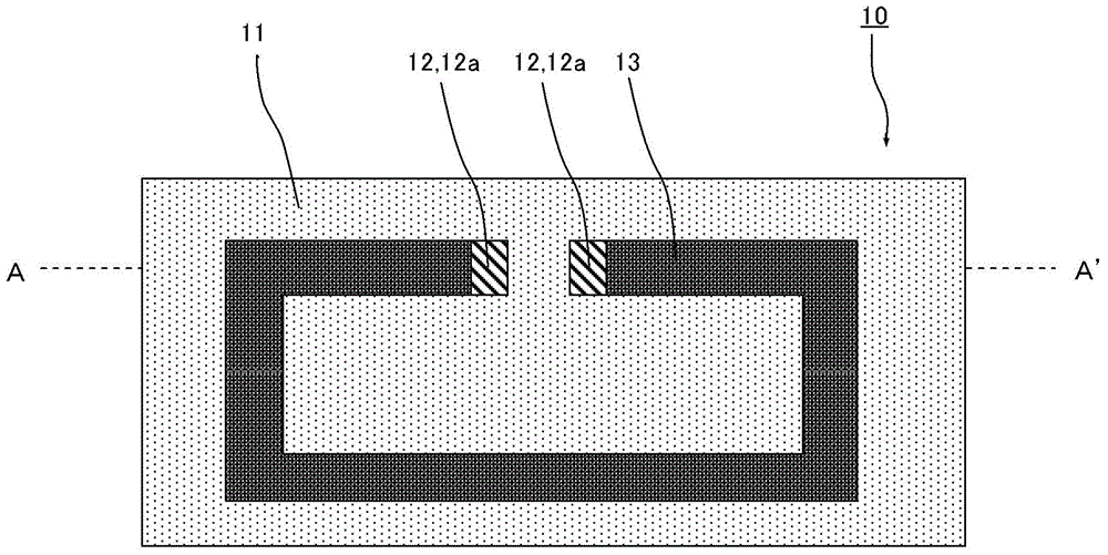
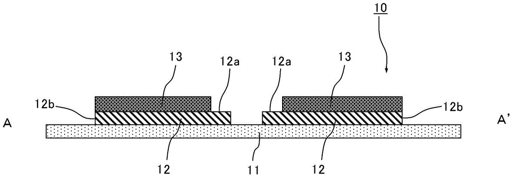
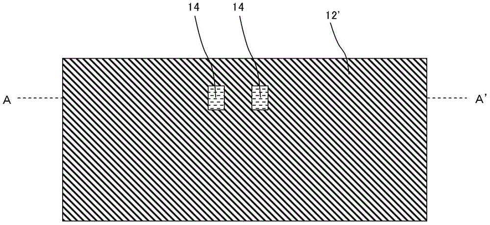
[0138] On the surface of the planar aluminum foil 12', the thickness after solvent volatilization is 2 μm Figure 10 and 11 As shown, an acid / alkali-resistant resist ink (manufactured by Asahi Chemical Laboratory Co., Ltd.: trade name U...


PUM

PropertyMeasurementUnit
Thicknessaaaaaaaaaa

Abstract

The invention provides a circuit substrate manufacturing method which be used for efficiently and easily forming a protective layer on the surface of a circuit-pattern-shaped metal foil and can restrain coating of a component mounting part by the protective layer through restraining offset of the protective layer from the position of the circuit-pattern-shaped metal foil. According to the circuit substrate manufacturing method, the circuit substrate is provided with the circuit-pattern-shaped metal foil, and the circuit-pattern-shaped metal foil is provided with a protective layer coating part which is coated by the protective layer and the component mounting part that is exposed from the metal foil. The circuit substrate manufacturing method comprises the steps of (1), a first step of forming a resist ink layer on a part which is used as the component mounting part on the planar metal foil surface; (2), a second step of forming the protective layer in a circuit pattern shape on the part except for the part used as the component mounting part on the planar metal foil surface; (3), a third step of forming the circuit-pattern-shaped metal foil through etching the planar metal foil in a manner that the resist ink layer and the protective layer are used as a mask; and (4), a fourth step of eliminating the resist ink layer.

Description

technical field [0001] This invention relates to the manufacturing method of the circuit board provided with the metal foil of a circuit pattern, and a circuit board. Background technique [0002] At present, in the manufacture of circuit boards such as RFID, copper or aluminum planar metal foils are laminated on both sides or one side of a resin film as a base with an adhesive, and then coated on the surface of the metal foil. A chemical-resistant ink or a photosensitive film is laminated, exposed, and developed to form a resist layer as a resist. [0003] Next, the metal foil at the portion where the resist layer is not formed is mainly etched with an acidic solution to form a circuit pattern. After etching, the resist layer that is no longer required is mainly removed with a weakly alkaline solution. [0004] Furthermore, after the circuit pattern is formed, the surface of the circuit pattern-shaped metal foil is coated with a solder resist or a protective layer for the...

Claims


Application Information

Patent Timeline
IPC IPC(8): H05K3/06
Inventor 田健吾猿渡昌隆
Owner TOYO ALUMINIUM KK
Learn More