A wafer thinning method
A wafer and filling layer technology, applied in the manufacturing of electrical components, circuits, semiconductor/solid-state devices, etc., can solve the problem of not being able to completely remove the silicon powder of the chip and affecting the production capacity.
Active Publication Date: 2019-01-22
SEMICON MFG INT (SHANGHAI) CORP
View PDF4 Cites 0 Cited by
- Summary
- Abstract
- Description
- Claims
- Application Information
AI Technical Summary
Problems solved by technology
In this way, not only the follow-up cleaning affects the production capacity, but also some customers refuse to accept this kind of wafer
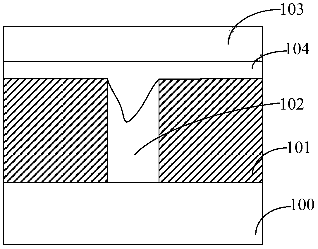
In order to reduce the entry of silicon powder into the chip, the previous method was to change the adhesive tape 103 to try to cover the gap (such as the dicing line 102) by replacing it with a more adhesive glue, but it still cannot solve the problem of silicon powder entering the chip from the side of the wafer. problem, and as shown in Figure 1A, when the thickness of the passivation film layer 101 is large, the aspect ratio of the slit (such as the cutting line 102) is very large, and the adhesive tape 103 can only cover the upper part of the slit, while the bottom area of the slit can still enter Silicon powder
In addition, the wafer or chip is cleaned several times in the follow-up, but the silicon powder in the chip cannot be completely removed.
Method used
View moreImage
Smart ImageViewing Examples
Examples
Embodiment Construction
Login to View More PUM
 Abstract
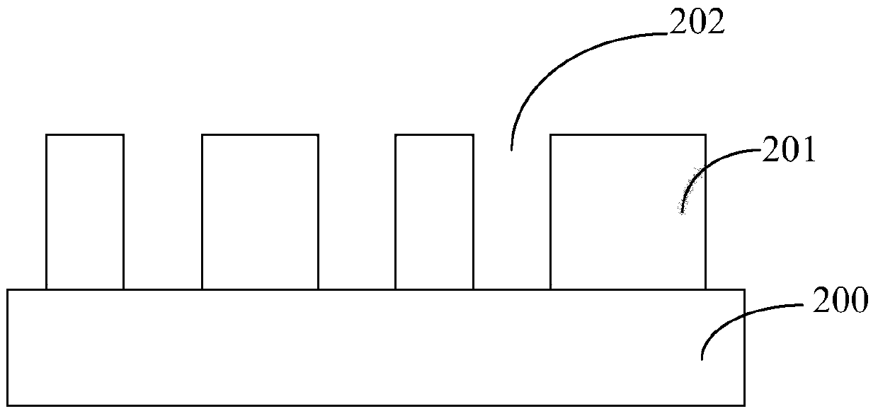
The invention provides a thickness reduction method for wafer. The method comprises: a semiconductor wafer is provided, a passivation layer is formed on the front side of the semiconductor wafer, and the passivation layer is etched to form a groove; a filling layer covering the wafer edge, the groove and the passivation layer is formed; the part, beyond the wafer edge and the groove are, of the filling layer is removed; an adhesive tape is formed on the passivation layer; wafer backside grinding is carried out on the wafer; the adhesive tape is removed; and the filling layer is removed. According to the method, because the filling layer is formed at gaps like a cutting lane and the wafer edge, when wafer backside grinding is carried out, silicon powder that is caused during the grinding process can not enter the chip either from the side of the wafer or from the bottom based on filling by the filling layer at the gaps and the wafer edge, so that a problem of silicon powder entrance into the chip during the wafer backside grinding process can be solved.
Description
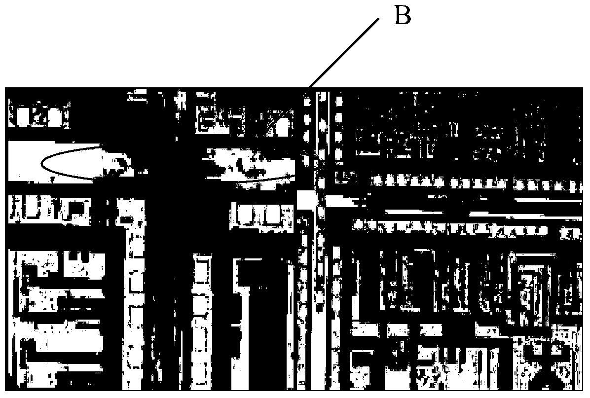
technical field The invention relates to the technical field of semiconductors, in particular to a wafer thinning method. Background technique At the back end of the semiconductor process, due to different process requirements, it is sometimes necessary to thin the wafer, that is, to perform backside grinding (backside grinding) to remove the excess matrix material on the back of the wafer to a certain thickness to reduce the backside of the wafer to A certain thickness, such as 19 mil, 12 mil, etc. For example, before integrated circuit packaging, two or more layers of chips are stacked together for system packaging. In order to adapt to the development trend of light and small integrated circuit chip packaging, people hope that the thickness of the wafer can be very thin. (that is, to manufacture ultra-thin wafers), so the wafers are thinned before the wafers are cut, such as thinning the wafers to 150um or even below 150um. As shown in FIG. 1A, the general process of w...
Claims
Login to View More Application Information
Patent Timeline
 Patent Type & Authority Patents(China)
IPC IPC(8): H01L21/02H01L21/312
Inventor 陈林徐超吴旭升
Owner SEMICON MFG INT (SHANGHAI) CORP
Features
- R&D
- Intellectual Property
- Life Sciences
- Materials
- Tech Scout
- Unparalleled Data Quality
- Higher Quality Content
- 60% Fewer Hallucinations
Learn More Browse by: Latest US Patents, China's latest patents, Technical Efficacy Thesaurus, Application Domain, Technology Topic, Popular Technical Reports.
© 2025 PatSnap. All rights reserved.Legal|Privacy policy|Modern Slavery Act Transparency Statement|Sitemap|About US| Contact US: help@patsnap.com


