Optical waveguide display module and electronic equipment

A display module and optical waveguide technology, which is applied in optics, nonlinear optics, instruments, etc., can solve the problems of low original light intensity, poor display uniformity of the display module, and inability to pass through the optical waveguide, etc., to improve display uniformity performance Effect

Active Publication Date: 2016-10-12
BOE TECH GRP CO LTD
View PDF11 Cites 5 Cited by
  • Summary
  • Abstract
  • Description
  • Claims
  • Application Information

AI Technical Summary

Problems solved by technology

[0010] When the liquid crystal layer is acted by an electric signal, it will show a scattering state, destroying the total reflection condition of the light, so that the light can pass through the optical waveguide transmission structure, otherwise the liquid crystal layer will be in a transmission state, and the light will be totally reflected inside the optical waveguide transmission structure. transmission mode, unable to pass through the optical waveguide
[0011] like figure 1 As shown, due to the attenuation effect of the optical waveguide transmission structure itself, as the distance between the pixel and the light source becomes farther and farther away, the intensity of the original light incident on the pixel becomes lower and lower, which results in applying the same electric current to different pixels. Signal, the brightness of the pixels is different, that is, the display uniformity of the display module is poor

Method used


Image

  • Optical waveguide display module and electronic equipment
  • Optical waveguide display module and electronic equipment
  • Optical waveguide display module and electronic equipment

Examples


Embodiment Construction

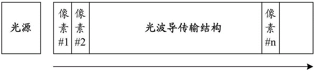
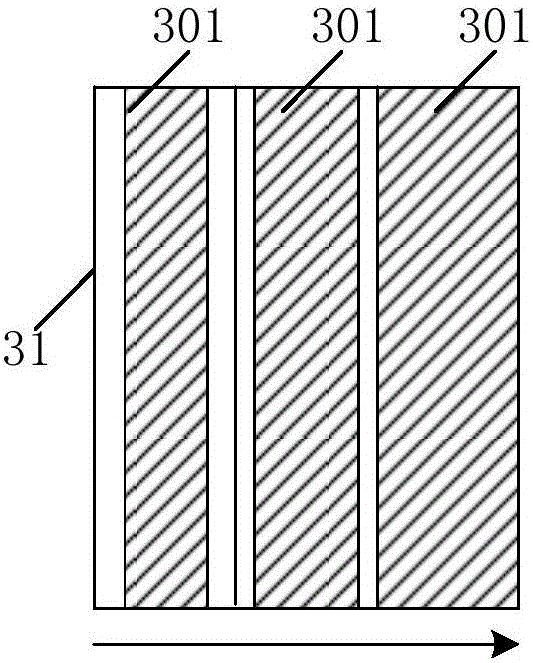
[0028] In the specific embodiment of the present invention, the scattering ability of the optical waveguide display module is designed according to the distance from the light source. The ability to destroy the total reflection condition), so as to make up for the display non-uniformity problem caused by light attenuation, and improve the display uniformity performance of the display module.

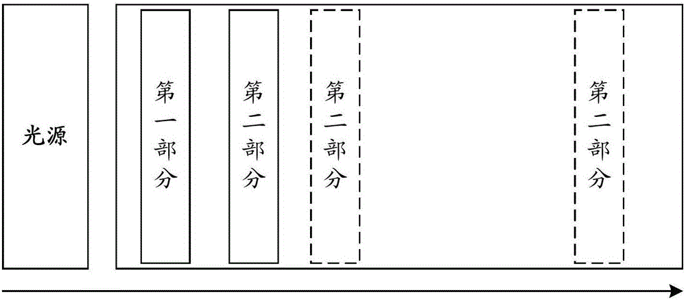
[0029] The optical waveguide display module according to the specific embodiment of the present invention has a display area, wherein the display area of ​​the optical waveguide display module includes two areas with the same area, and the voltage of the electrical signal applied to the pixel electrode is equal to At the same time, the scattering ability of the first part of the optical waveguide display module is weaker than the scattering ability of the second part of the optical waveguide display module, such as figure 2 As shown, the first part of the optical waveguide display modul...


PUM


Abstract

The invention discloses an optical waveguide display module and electronic equipment, and aims at improving the display uniformity. The optical waveguide display module is provided with a display area, the display area of the optical waveguide display module comprises two regions with the same area, and when voltages of electrical signals applied by pixel electrodes are the same, the scattering capacity of the first part of the optical waveguide display module is weaker than that of the second part of the optical waveguide display module; the first part of the optical waveguide display module corresponds to the portion of the region, closer to a light source, in the two regions, and the second part of the optical waveguide display module is the portion of the region, farther to the light source, in the two regions. By means of the optical waveguide display module and the electronic equipment, the display uniformity of the optical waveguide display module is improved.

Description

technical field [0001] The invention relates to display technology, in particular to an optical waveguide display module and electronic equipment capable of improving display uniformity. Background technique [0002] With the continuous progress of display technology, new display technologies are constantly being proposed and implemented by people, and transparent display products are such a new type of display products. [0003] During the working process of the transparent display device, the user can clearly see the scene behind it through the transparent display device. The transparent display device is favored by more and more people because of its transparent appearance, and gradually It has become a trend in the development of display technology and has been applied to products such as shopping mall cabinets, smart glasses, and smart helmets. [0004] Optical waveguide transparent display is a kind of transparent display technology, which has higher light transmittan...

Claims


Application Information

Patent Timeline
Patent Type & Authority Applications(China)
IPC IPC(8): G02F1/1333
CPCG02F1/1333G02F1/1334G02F1/133615G02F1/134309C09K19/542C09K2019/548G02F1/133553G02F1/137G02F2201/121G02F2201/122G02F2201/123G02F1/13775
Inventor 李鑫
Owner BOE TECH GRP CO LTD
Why Eureka
Try Eureka