A kind of indium gallium phosphide heterojunction bipolar transistor and its manufacturing method

A heterojunction bipolar, indium gallium phosphide technology, applied in semiconductor/solid-state device manufacturing, semiconductor devices, electrical components, etc., can solve problems such as low linearity and poor reliability, achieve high energy density, improve linearity, The effect of good linearity

Active Publication Date: 2019-02-12
SUZHOU LIANG DONGXIN MICROELECTRONICS CO LTD
View PDF4 Cites 0 Cited by
  • Summary
  • Abstract
  • Description
  • Claims
  • Application Information

AI Technical Summary

Problems solved by technology

[0004] The purpose of the present invention is to overcome the technical problems of low linearity and poor reliability of existing aluminum gallium arsenic heterojunction bipolar transistors, and provide an indium gallium phosphide heterojunction bipolar transistor and a manufacturing method thereof, which can Effectively Improving the Linearity and Reliability of Heterojunction Bipolar Transistors

Method used


Image

  • A kind of indium gallium phosphide heterojunction bipolar transistor and its manufacturing method
  • A kind of indium gallium phosphide heterojunction bipolar transistor and its manufacturing method
  • A kind of indium gallium phosphide heterojunction bipolar transistor and its manufacturing method

Examples


Embodiment

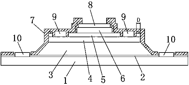
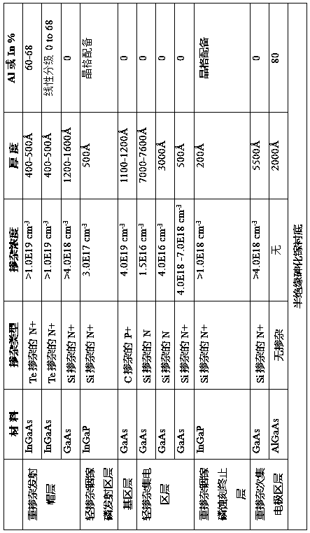
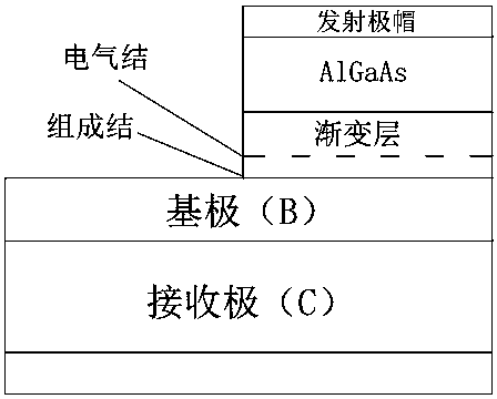
[0028] Embodiment: a kind of indium gallium phosphide heterojunction bipolar transistor of this embodiment, such as figure 1 As shown, from bottom to top, it includes substrate, heavily doped sub-collector layer 1, heavily doped InGaP etch stop layer 2, lightly doped collector layer 3, base layer 4, lightly doped indium The gallium-phosphorus emitter layer 5 and the heavily doped emitter cap layer 6, the heavily doped emitter cap layer 6 is provided with an emitter ohmic contact 8, the base layer 4 is provided with a base ohmic contact 9, and the heavily doped sub-collector The collector ohmic contact 10 is arranged on the region layer 1, and the polar edge of the lightly doped indium gallium phosphide emitter layer 5 is passivated, and the distance between the edge of the lightly doped indium gallium phosphide emitter layer mesa and the edge of the base layer is 0.5 -1µm, the surface of the indium gallium phosphide heterojunction bipolar transistor is provided with a silicon ...


PUM


Abstract

The invention discloses an indium-gallium-phosphorus heterojunction bipolar type transistor and a manufacturing method therefor. The indium-gallium-phosphorus heterojunction bipolar type transistor comprises a substrate, a heavily-doped secondary collector region layer, a heavily-doped indium-gallium-phosphorus etching stop layer, a lightly-doped collector region layer, a base region layer, a lightly-doped indium-gallium-phosphorus emitter region layer and a heavily-doped emission cap layer from the bottom up in sequence. The linearity and the reliability of the indium-gallium-phosphorus heterojunction bipolar type transistor can be effectively improved.

Description

technical field [0001] The invention relates to the technical field of heterojunction bipolar transistors, in particular to an indium gallium phosphide heterojunction bipolar transistor and a manufacturing method thereof. Background technique [0002] Heterojunction bipolar transistor (HBT) has good power added efficiency (PAE) and noise figure characteristics, its characteristic frequency ft is high, high base doping will lead to large fmax and high Early Voltage (Early Voltage) , a controllable high breakdown voltage yields high power density, and a low “knee” voltage yields high power efficiency. The preparation technology of heterojunction bipolar transistors, especially the epitaxial growth technology has promoted the development and application of semiconductor devices such as heterojunction bipolar transistors. [0003] At present, the commonly used heterojunction bipolar transistor is aluminum gallium arsenide (AlGaAs) heterojunction bipolar transistor, but the line...

Claims


Application Information

Patent Timeline
Patent Type & Authority Patents(China)
IPC IPC(8): H01L29/08H01L21/331H01L29/737
CPCH01L29/0804H01L29/66242H01L29/7371
Inventor 汪耀祖
Owner SUZHOU LIANG DONGXIN MICROELECTRONICS CO LTD
Why Eureka
Try Eureka