Ultrathin packaging component and manufacturing technique thereof

A manufacturing process and packaging technology, applied in the field of ultra-thin packaging and its manufacturing process, can solve the problems of unguaranteed packaging reliability, high cost, large thickness, etc., and achieve shortened design cycle, I/O intensive, Realize the effect of interconnection

Inactive Publication Date: 2016-08-17
GUANGDONG CHIPPACKING TECH
View PDF4 Cites 3 Cited by
  • Summary
  • Abstract
  • Description
  • Claims
  • Application Information

AI Technical Summary

Problems solved by technology

[0004] The traditional QFN / DFN mainly has the following shortcomings: first, the design and production cycle is long, and the cost is relatively high; second, the arrangement of bumps and the density of I / O are limited by the frame design and frame manufacturing process; After corrosion and thinning, there is a risk of sliding in the mold, and the reliability of the packaging cannot be guaranteed; Fourth, the thickness of traditional QFN / DFN products is still relatively large, which cannot meet the needs of current portable devices for small-volume, high-density packaging

Method used


Image

  • Ultrathin packaging component and manufacturing technique thereof
  • Ultrathin packaging component and manufacturing technique thereof
  • Ultrathin packaging component and manufacturing technique thereof

Examples


Embodiment Construction

[0040] The present invention will be described in further detail below in conjunction with the accompanying drawings.

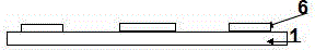
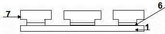
[0041] refer to Figure 12 As shown, the present invention discloses an ultra-thin package, including a plastic package 4 and a chip 3 packaged in the plastic package 4, a silver-plated layer 5, a NiPdAu-plated layer 6, a copper connection layer 7 and a bonding wire 8. The chip 3, the silver-plated layer 5, the copper connection layer 7, the NiPdAu-plated layer 6 and the bonding wire 8 constitute the power supply and the signal channel of the circuit, and there are multiple copper connection layers 7, and each copper connection layer 7 The upper surface of the upper surface is provided with a silver-plated layer 5, and the lower surface is provided with a NiPdAu-plated layer 6. The plurality of silver-plated layers 5 are independent of each other, and the chip 3 is arranged on a part of the silver-plated layer 5. The silver layer 5 is connected to the chip 3...


PUM

PropertyMeasurementUnit
thicknessaaaaaaaaaa

Abstract

The invention discloses an ultrathin packaging component including a plastic packaging body, a chip, silver coating layers, NiPdAu coating layers, a plurality of copper connecting layers and bonding lines. The chip, the silver coating layers, the NiPdAu coating layers, the copper connecting layers and the bonding lines are all packaged in the plastic packaging body and form a power supply and signal channel of a circuit. One of the silver coating layers and one of the NiPdAu coating layer are arranged on the upper surface and the lower surface of each copper connecting layer. The silver coating layers are independent from each other. The chip is arranged on a part of the silver coating layers. The part of silver coating layer without the chip are connected with the chip by the bonding lines. As electroplating and film pasting can be avoided, the manufacturing cost can be largely reduced, and the product is more competitive. The invention also discloses a manufacturing technique of the ultrathin packaging component. The product manufacturing process can be conducted with a common framework, and a framework carrier does not need to be processed too much, so that the design period is shortened, the cost is reduced, the interconnection between the chip and the carrier is better achieved, and I/O is denser.

Description

technical field [0001] The invention belongs to the technical field of integrated circuit packaging, and in particular relates to an ultra-thin package and a manufacturing process thereof. Background technique [0002] Integrated circuit QFN (Quad Flat No-lead Package) and DFN (Dual Flat Package, double-sided pin flat package) in recent years with the communication equipment (such as base stations, switches), smart phones, portable Devices (such as tablet computers), wearable devices (such as smart watches, smart glasses, smart bracelets, etc.) Packaging of large-scale integrated circuits with equal electrical requirements. [0003] QFN / DFN effectively utilizes the packaging space of the lead pins, thereby greatly improving the packaging efficiency. Due to the short lead wires, small plastic package size and thin package body, the package can reduce the volume of the CPU by 30%-50%, and has good heat dissipation performance at the same time. [0004] The traditional QFN / D...

Claims


Application Information

Patent Timeline
Patent Type & Authority Applications(China)
IPC IPC(8): H01L23/522H01L21/60
CPCH01L2224/48091H01L2224/48247H01L2924/00014
Inventor 宋波梁大钟施保球刘兴波
Owner GUANGDONG CHIPPACKING TECH
Why Eureka
Try Eureka