Processing method of round chips and semiconductor wafer

A processing method and chip technology, which are applied in the process of producing decorative surface effects, metal material coating process, decorative arts, etc., can solve problems such as the difficulty of equipment research and development, achieve high dicing efficiency, improve cutting efficiency, The effect of reduced cutting stroke

Active Publication Date: 2016-08-10
THE 13TH RES INST OF CHINA ELECTRONICS TECH GRP CORP
View PDF8 Cites 0 Cited by
  • Summary
  • Abstract
  • Description
  • Claims
  • Application Information

AI Technical Summary

Problems solved by technology

However, due to technical reasons and the difficulty of developing related equipment, the current DRIE process does not directly implement the MEMS wafer scribing process alone.

Method used


Image

  • Processing method of round chips and semiconductor wafer
  • Processing method of round chips and semiconductor wafer
  • Processing method of round chips and semiconductor wafer

Examples


Embodiment Construction

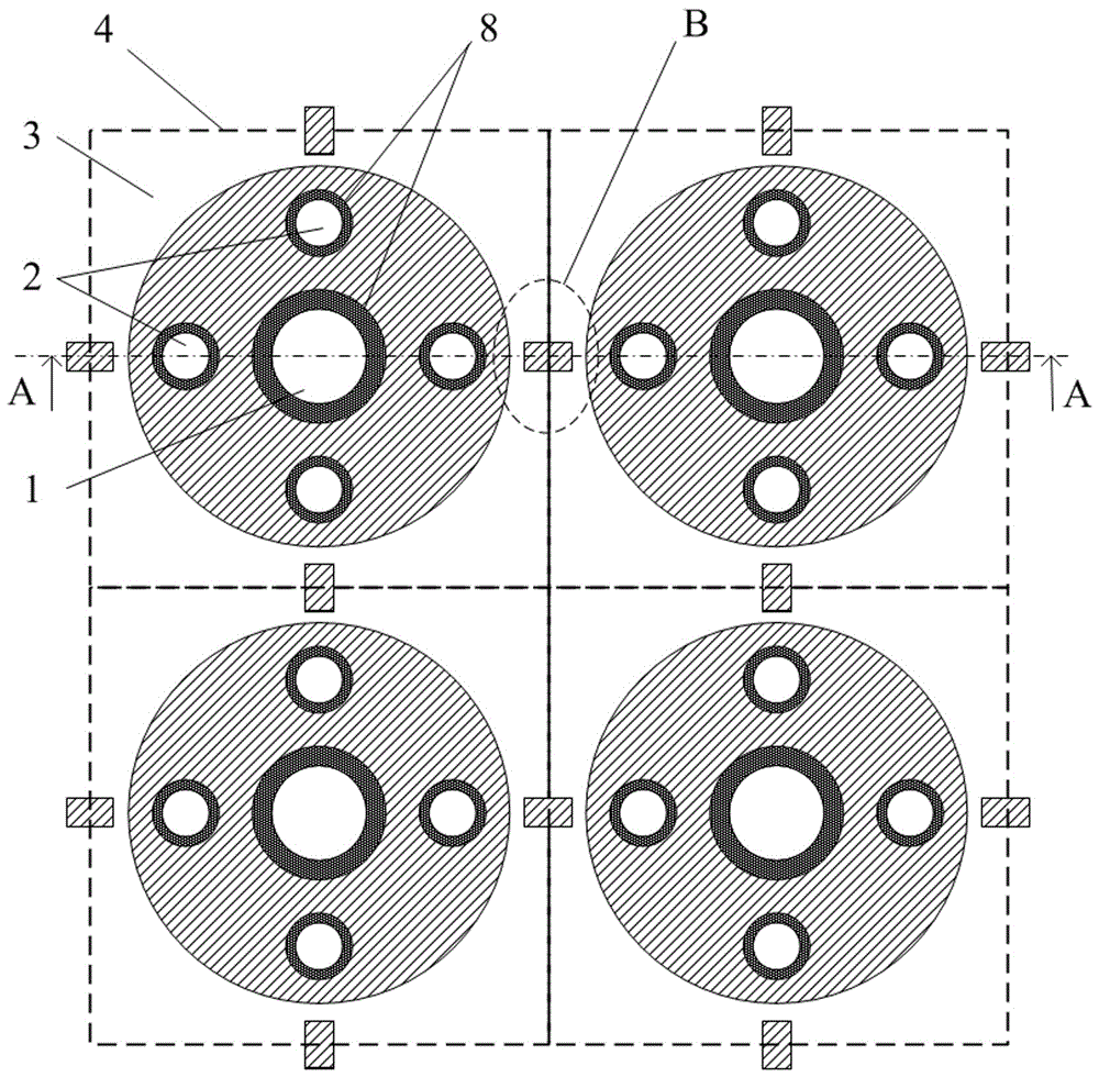
[0030] The invention provides a method for processing a circular chip and a wafer capable of cutting and separating the circular chip. The scribing process is simple and the difficulty is small. The grinding wheel dicing machine can be used to realize chip cutting and separation. At the same time, it has the advantages of small scribing stroke, high cutting efficiency, little damage to the appearance of the chip after dicing, and high mechanical strength.

[0031] Taking the preparation of a MEMS circulator chip as an example below, the processing method and wafer of the present invention will be further described in conjunction with the accompanying drawings.

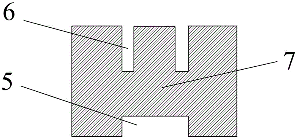
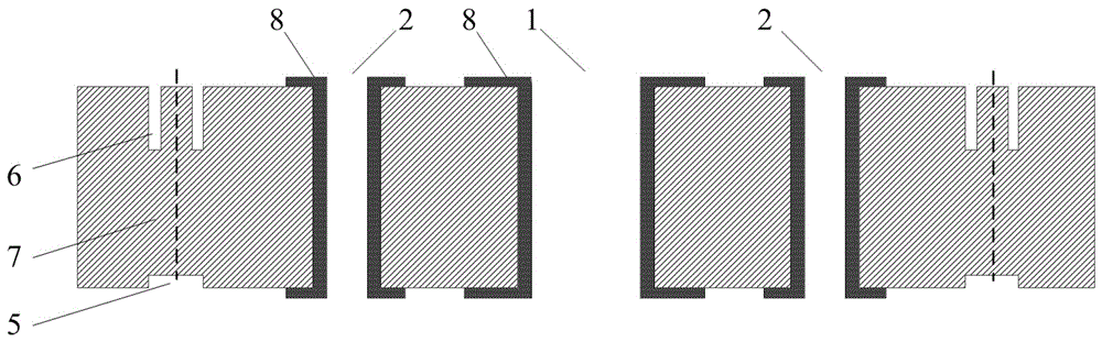
[0032] The MEMS circulator is a circular chip structure, and its processing method includes the following steps: the first step is to prepare the back cutting groove 5. The preparation of the back cutting groove 5 is formed by an RIE etching process, and a silicon wet etching process can also be used to cut the groove. ...


PUM

PropertyMeasurementUnit
widthaaaaaaaaaa
depthaaaaaaaaaa
lengthaaaaaaaaaa

Abstract

The invention relates to the technical field of processing method of semiconductor wafer chips, and in particular to the field of scribing technology of MEMS round chips. The invention particularly discloses a processing method of round chips and a semiconductor wafer. The round chip is obtained by making through holes in the wafer. Chips are connected only through support beams with small grooves, so that the chips can be separated only by cutting off the support beams, and the scribing difficulty is low. The cutting can be realized by adopting common abrasion wheels. The method has the advantages of simple process, low cost and high efficiency. The obtained separated chips have the advantages of good appearances, high finished product ratio and high mechanical strength.

Description

technical field [0001] The invention relates to the technical field of processing methods for semiconductor wafer chips, in particular to the technical field of dicing MEMS circular chips. Background technique [0002] Traditional MEMS chips are all square or rectangular chips. In some fields, due to the performance requirements of the package or the product itself, it is necessary to make the MEMS chip into a circular shape. At present, in the field of MEMS wafer scribing, there are mainly grinding wheel scribing and laser scribing. Grinding wheel dicing is the most widely used cutting technology at present. Its mechanism is mechanical grinding. Grinding wheel dicing is a linear cutting process, which cannot realize the separation of circular chips. , and due to the mechanical contact during the cutting process of the grinding wheel, the edges of MEMS chips are very prone to edge chipping, especially the edge chipping on the back of the chip; while laser scribing equipment...

Claims


Application Information

Patent Timeline
Patent Type & Authority Applications(China)
IPC IPC(8): B81C1/00
CPCB81C1/00865B81C1/00873B81C1/00896
Inventor 任霄峰胥超何洪涛徐永青
Owner THE 13TH RES INST OF CHINA ELECTRONICS TECH GRP CORP
Why Eureka
Try Eureka