Solar cell based on silicon nanowires
A technology of solar cells and silicon nanowires, which is applied in the field of solar cells, can solve problems such as the difficulty in reducing the light reflection coefficient of the substrate, the difficulty in obtaining high-quality suede light trapping, and the increase in the density of substrate surface defects, so as to improve energy conversion Efficiency, good light trapping effect, effect of improving passivation performance
- Summary
- Abstract
- Description
- Claims
- Application Information
AI Technical Summary
Problems solved by technology
Method used
Image

Examples
Embodiment 1
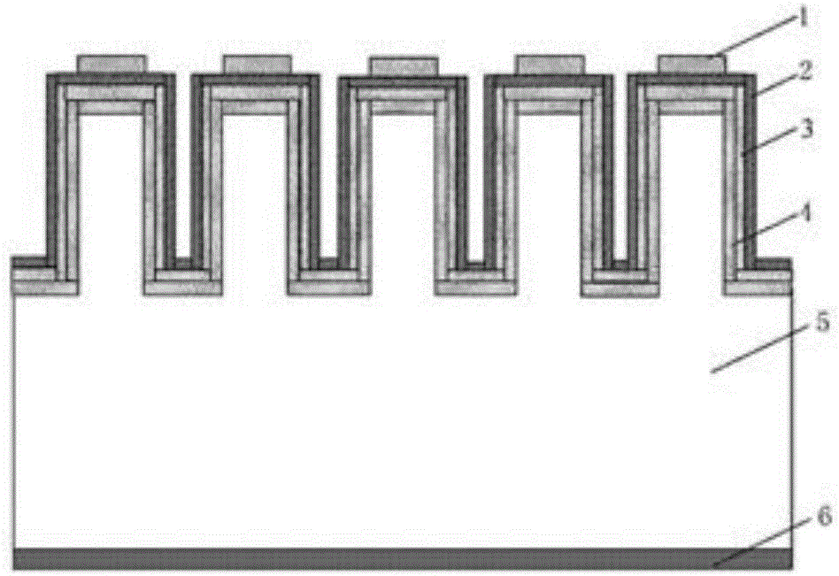
[0016] The solar cell of this example includes a positive electrode 1, an indium tin oxide transparent conductive film 2, an N-type amorphous silicon layer 3, an i-type layer 4, a P-type silicon substrate 5, and a back electrode 6, wherein the back electrode 6 is located on the P-type silicon substrate. On the back of the substrate 5, the upper surface of the P-type silicon substrate 5 adopts a nanowire array structure, and the i-type layer 4, the N-type amorphous silicon layer 3 and the indium tin oxide transparent conductive film 2 are sequentially stacked on the surface of the nanowire array structure, The positive electrode 1 is arranged on the top of the nanowire array structure. The positive electrode 1 is made of a Ti / Pd / Ag multilayer metal material with a thickness of 20nm / 20nm / 40nm; the thickness of the N-type amorphous silicon layer 3 and the i-type layer 4 are both 10nm; the silicon nanowire array , the diameter of each silicon nanowire is 40nm, and the length is 5 ...
Embodiment 2
[0018] The structure of the solar cell of this example is the same as that of Embodiment 1, that is, the solar cell using a silicon nanowire array structure, and its parameters change as follows:
[0019] Both the N-type amorphous silicon layer 3 and the i-type layer 4 have a thickness of 30 nm; in the silicon nanowire array, each silicon nanowire has a diameter of 60 nm and a length of 8 μm; the P-type silicon substrate 5 has a thickness of is 300 μm.
Embodiment 3
[0021] The structure of the solar cell of this example is the same as that of Embodiment 1, that is, the solar cell using a silicon nanowire array structure, and its parameters change as follows:
[0022] Both the N-type amorphous silicon layer 3 and the i-type layer 4 have a thickness of 50 nm; in the silicon nanowire array, each silicon nanowire has a diameter of 80 nm and a length of 10 μm; the P-type silicon substrate 5 has a thickness of is 400 μm.
[0023] The manufacturing method of the solar cell of the embodiment 1-3 is: first form the nanowire array structure by dry etching or wet etching on the upper surface of the P-type silicon substrate 5; Depositing and forming microcrystalline silicon intrinsic layer, amorphous silicon germanium intrinsic layer, amorphous silicon intrinsic layer and microcrystalline silicon carbide intrinsic layer by PECVD method to form i-type layer 4, and then depositing by PECVD method to form N-type Amorphous silicon layer 3, forming an in...
PUM
| Property | Measurement | Unit |
|---|---|---|
| thickness | aaaaa | aaaaa |
| diameter | aaaaa | aaaaa |
| length | aaaaa | aaaaa |
Abstract
Description
Claims
Application Information
 - R&D
- Intellectual Property
- Life Sciences
- Materials
- Tech Scout
- Unparalleled Data Quality
- Higher Quality Content
- 60% Fewer Hallucinations
Browse by: Latest US Patents, China's latest patents, Technical Efficacy Thesaurus, Application Domain, Technology Topic, Popular Technical Reports.
© 2025 PatSnap. All rights reserved.Legal|Privacy policy|Modern Slavery Act Transparency Statement|Sitemap|About US| Contact US: help@patsnap.com