Metal wire grating brightness enhance film for display backlight and preparation method for metal wire grating brightness enhance film
A technology of metal wire grid and brightness enhancement film, which is applied in the field of metal wire grid brightness enhancement film for display backlight and its preparation, can solve the problems of complex preparation process of brightness enhancement film and the inability of the product to meet the requirements of backlight display, and achieve P-state wear. Increased transmittance, optimized structure, and improved versatility
- Summary
- Abstract
- Description
- Claims
- Application Information
AI Technical Summary
Problems solved by technology
Method used
Image


Examples
preparation example Construction
[0032] see figure 2 , figure 2 It is a schematic flow chart of a preferred embodiment of a method for preparing a metal wire grid brightness enhancement film for a display backlight in the present invention, and the method includes but is not limited to the following steps.
[0033] Step S100, coating a photoresist on the surface of the substrate.
[0034] In step S100, firstly, a flexible substrate is selected as the substrate of the metal wire grid, wherein the flexible substrate is usually made of flexible materials such as polymer or PET, which is convenient to be combined with the existing roll-to-roll equipment process, and has many advantages. Good light transmission, can be used for TFT-LCD display. In addition, the photoresist should have low viscosity for easy separation from the roll-to-roll imprint mold, and have good mechanical properties after curing with sufficient support.
[0035] Step S110 , forming a nanometer-sized photoresist grating structure on the ...
Embodiment 1
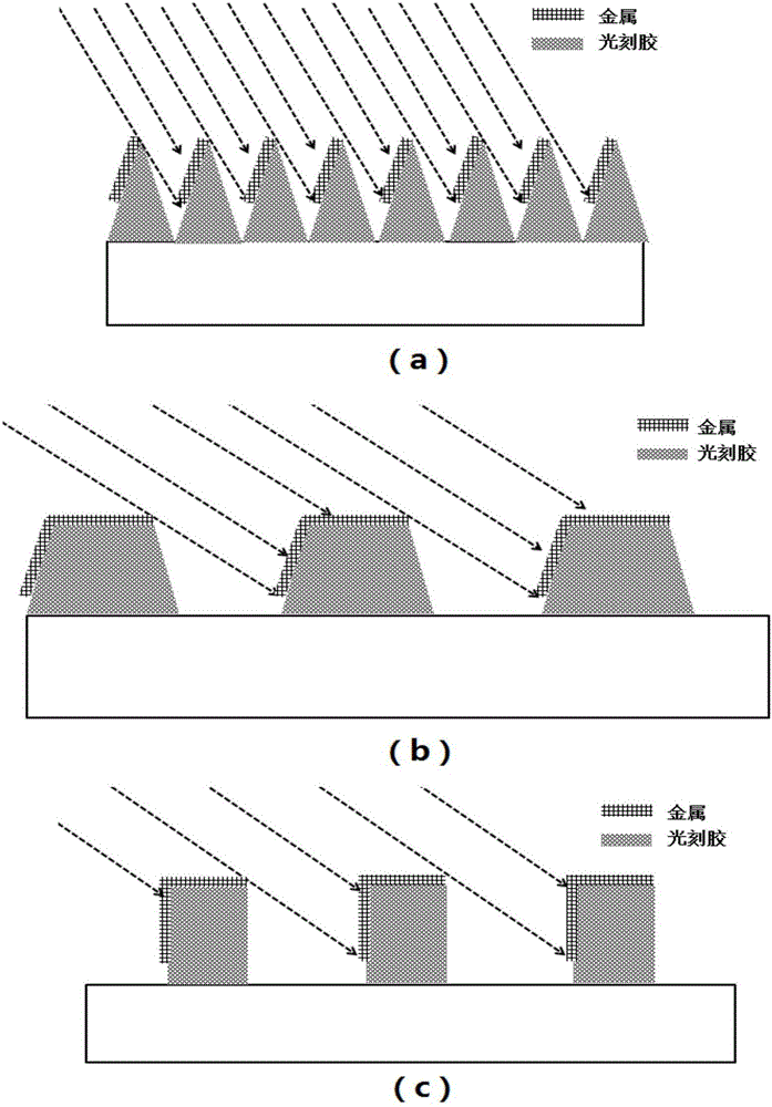
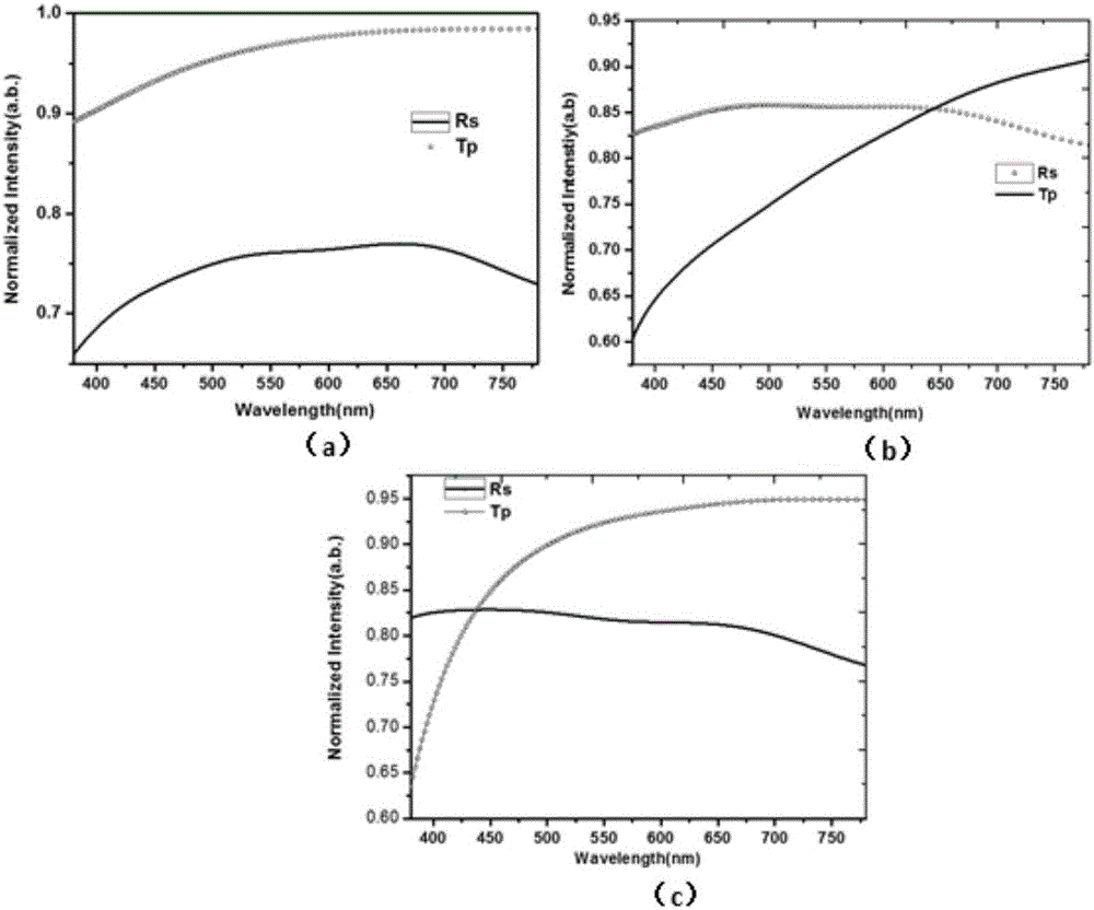
[0044] A photoresist grating structure with a triangular cross-section is prepared by a roll-to-roll nanoimprinting method, and then metal is deposited on one side of the triangular prism by pointing oblique evaporation. The specific structure is as Figure 4 As shown in (a), the photoresist grating period is about 100-300nm, the grating width is 100-200nm, the grating thickness is 100-200nm, and the thickness of the metal layer is 10-100nm. Figure 5 (a) is a photoresist grating structure with a triangular cross-section through FDTD to simulate the trend curve of Tp and Rs with wavelength, wherein Rs is greater than 0.9, Tp is about 0.7, and the minimum value is T=0.5*0.7*(1+0.9) =66.5%, which is a gain of about 58% relative to common absorbing polarizers (the light transmittance of common absorbing polarizers is about 42%).
Embodiment 2
[0046] A photoresist grating structure with a trapezoidal cross-section is prepared by a roll-to-roll nanoimprinting method, and then metal is deposited on the top surface and one side of the trapezoidal prism by means of directed oblique evaporation. The specific structure is as Figure 4 As shown in (b), the period of the photoresist grating is about 100-300nm, the grating width is 100-200nm, the grating thickness is 100-200nm, and the thickness of the metal layer is 10-100nm. Figure 5 (b) is a photoresist grating structure with a trapezoidal cross-section through FDTD simulation of Tp, Rs variation trend curves with wavelength, wherein Rs is about 0.8, Tp is greater than 0.6, and the minimum value T=0.5*0.6*(1+0.8 )=54%, which is about 29% relative to the gain of ordinary absorbing polarizers.
PUM
| Property | Measurement | Unit |
|---|---|---|
| width | aaaaa | aaaaa |
| thickness | aaaaa | aaaaa |
| width | aaaaa | aaaaa |
Abstract
Description
Claims
Application Information
 - R&D
- Intellectual Property
- Life Sciences
- Materials
- Tech Scout
- Unparalleled Data Quality
- Higher Quality Content
- 60% Fewer Hallucinations
Browse by: Latest US Patents, China's latest patents, Technical Efficacy Thesaurus, Application Domain, Technology Topic, Popular Technical Reports.
© 2025 PatSnap. All rights reserved.Legal|Privacy policy|Modern Slavery Act Transparency Statement|Sitemap|About US| Contact US: help@patsnap.com