A method for optical visualization of two-dimensional atomic crystal materials on substrate surfaces

A two-dimensional atomic crystal, substrate surface technology, applied to two-dimensional atomic crystal materials, directly observed under a magnifying glass or even with the naked eye, graphene in the field of ordinary optical microscope, can solve the problem of inability to remove, affect graphene measurement and application, pollution Graphene surface and other issues

Active Publication Date: 2018-12-28
TSINGHUA UNIV
View PDF1 Cites 0 Cited by
  • Summary
  • Abstract
  • Description
  • Claims
  • Application Information

AI Technical Summary

Problems solved by technology

However, these auxiliary molecules need to be deliberately removed or even cannot be removed, which will contaminate the surface of graphene and affect the further measurement and application of graphene.
[0006] So far, there has not been a method with strong applicability (suitable for two-dimensional atomic crystal materials on various substrate surfaces, especially graphene), strong controllability, repeatable and non-polluting methods to realize two-dimensional atomic crystal materials Direct observation under ordinary optical microscopes enables the localization, characterization and manipulation of two-dimensional atomic crystal materials

Method used


Image

  • A method for optical visualization of two-dimensional atomic crystal materials on substrate surfaces
  • A method for optical visualization of two-dimensional atomic crystal materials on substrate surfaces
  • A method for optical visualization of two-dimensional atomic crystal materials on substrate surfaces

Examples


Embodiment 1

[0027] Embodiment 1, using water vapor to assist the optical visualization of graphene on a copper substrate

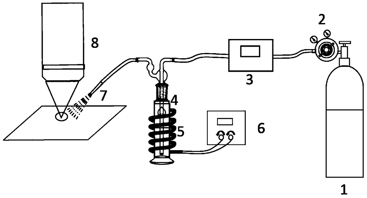
[0028] Specific observation devices such as figure 1 As shown, first adjust the voltage source voltage to 100V, heat the water in the container through the heating belt, when the water is heated to warm water, reduce the power supply voltage to 50V and keep it, then adjust the pressure reducing valve to release argon and adjust the gas flowmeter to At 200sccm, argon gas enters the container, bringing out water vapor and ejecting it from the nozzle. Place the sample on the stage of the microscope. When the water vapor is sprayed on the surface of the sample, the water vapor will condense into water droplets and be observed directly through the microscope.

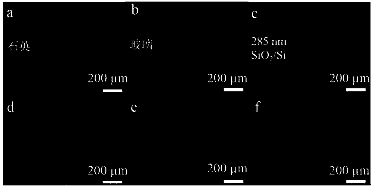
[0029] In this embodiment, the optical photographs before and after water vapor spraying on the copper substrate surface with graphene are as follows: figure 2 As shown, the differences in morphology, density, an...

Embodiment 2

[0032] Embodiment 2, using water vapor to assist in realizing the optical visualization of graphene on a quartz substrate

[0033] The specific observation device is the same as in Example 1. First, the graphene is transferred to the surface of the quartz substrate, the voltage source is adjusted to 100V, and the water in the container is heated by the heating belt. When heated to warm water, the power supply voltage is reduced to 50V and maintained. Then adjust the pressure reducing valve to release the argon and adjust the gas flow meter to 200 sccm, the argon enters the container, brings out the water vapor and sprays it out from the nozzle. The quartz substrate transferred with graphene is placed on the stage of the microscope in the device. When the water vapor is sprayed on the surface of the sample, the water vapor condenses into water droplets and is directly observed through the microscope.

[0034] In this embodiment, the optical photographs before and after water va...

Embodiment 3

[0036] Embodiment 3, using water vapor to assist in realizing the optical visualization of graphene on a glass substrate

[0037] The specific observation device is the same as in Example 1. First, the graphene is transferred to the surface of the glass substrate, the voltage source is adjusted to 100V, and the water in the container is heated by the heating belt. When heated to warm water, the power supply voltage is reduced to 50V and maintained. Then adjust the pressure reducing valve to release the argon and adjust the gas flow meter to 200 sccm, the argon enters the container, brings out the water vapor and sprays it out from the nozzle. The glass substrate transferred with graphene is placed on the stage of the microscope in the device. When the water vapor is sprayed on the surface of the sample, the water vapor condenses into water droplets and is directly observed through the microscope.

[0038] In the present embodiment, the optical photographs before and after wate...


PUM

PropertyMeasurementUnit
strengthaaaaaaaaaa
electrical resistivityaaaaaaaaaa

Abstract

The invention provides a method for realizing optical visualization of a two-dimensional atomic crystal material on a substrate surface. According to the method, a sample to be detected, whose surface contains a two-dimensional atomic crystal material, is placed on the objective table of an optical microscope or is directly placed under a magnifying lens, then water steam is sprayed on the surface of the sample, and thus the two-dimensional atomic crystal material on the substrate surface is clearly visible under the optical microscope. Moreover, the method can also distinguish the single layer and multi-layer two-dimensional atomic crystal material areas. The method does not need pricy or complicated equipment, the operation is simple, the cost is low, the pretreatment of sample is not needed; only under the assistance of water steam, two-dimensional atomic crystal materials such as graphene can be directly observed and positioned by common optical microscope, amplifying lens, or even naked eyes; the sample surface will not be contaminated after water drops are evaporated; the subsequent operation and application are not influenced; thus the method can be performed repeatedly, the method is green and environment-friendly, and the research on two-dimensional atomic material such as graphene and manufacture of related devices become easier.

Description

technical field [0001] The invention relates to a method for directly observing two-dimensional atomic crystal materials on various substrate surfaces, especially graphene, under an ordinary optical microscope, a magnifying glass or even naked eyes, and belongs to the technical field of material characterization analysis. Background technique [0002] Nanomaterials refer to materials in which at least one dimension in three-dimensional space is in the nanoscale range (1-100nm) or composed of them as constituent units. Among them, two-dimensional materials refer to materials that electrons can move freely at the nanoscale in two dimensions. Two-dimensional materials were proposed following the successful separation of monoatomic layer graphene materials by the Geim group in the United Kingdom in 2004. Due to the outstanding characteristics of graphene, graphene has attracted great interest in both theoretical research and application fields. Subsequent other two-dimensional ...

Claims


Application Information

Patent Timeline
Patent Type & Authority Patents(China)
IPC IPC(8): G01N21/00
CPCG01N21/00
Inventor 张莹莹夏凯伦
Owner TSINGHUA UNIV
Why Eureka
Try Eureka