Manufacturing method of TFT substrate and prepared TFT substrate

一种制作方法、基板的技术,应用在半导体/固态器件制造、仪器、半导体器件等方向,能够解决TFT电性稳定性劣化、多光罩次数、生产成本高等问题,达到减少光罩次数、提高生产效率、生产成本低的效果

Active Publication Date: 2016-06-01
TCL CHINA STAR OPTOELECTRONICS TECH CO LTD
View PDF4 Cites 31 Cited by
  • Summary
  • Abstract
  • Description
  • Claims
  • Application Information

AI Technical Summary

Problems solved by technology

Since the channel of the top-gate coplanar TFT is easily affected by the illumination from below, the electrical stability of the TFT will be deteriorated, so a light-shielding layer needs to be added in this area
However, the traditional FFS display mode array substrate manufacturing method requires more photomasks, the process is more complicated, and the production cost is higher.

Method used


Image

  • Manufacturing method of TFT substrate and prepared TFT substrate
  • Manufacturing method of TFT substrate and prepared TFT substrate
  • Manufacturing method of TFT substrate and prepared TFT substrate

Examples


Embodiment Construction

[0048] In order to further illustrate the technical means adopted by the present invention and its effects, the following describes in detail in conjunction with preferred embodiments of the present invention and accompanying drawings.

[0049] see figure 1 , the invention provides a kind of manufacturing method of TFT substrate, comprises the following steps:

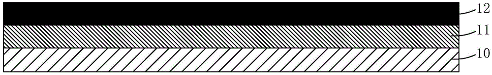
[0050] Step 1, such as figure 2 As shown, a substrate 10 is provided, and a transparent conductive film 11 and a light-shielding film 12 are sequentially deposited on the substrate 10 .

[0051] Specifically, the substrate 10 is a transparent substrate, preferably a glass substrate.

[0052] Specifically, in the step 1, before depositing the transparent conductive film 11 on the substrate 10, the substrate 10 needs to be cleaned.

[0053] Specifically, the material of the transparent conductive film 11 is a transparent conductive metal oxide, such as indium tin oxide (ITO), indium zinc oxide (IZO), aluminum tin oxi...


PUM


Abstract

The invention provides a manufacturing method of a TFT substrate and a prepared TFT substrate. According to the manufacturing method of the TFT substrate, based on the characteristic of high visible light transmittance of a transparent metal oxide semiconductor material and doping processing is performed on a transparent metal oxide semiconductor, so that a transparent metal oxide conductor can be obtained, and at the same time, an active layer and a pixel electrode are formed, and therefore, the number of the times of photo masking can be decreased, production efficiency can be improved, and production cost can be reduced; in addition, based on only one semi-transparent photo mask, exposure and etching are performed, so that a common electrode, and a stack light shielding layer formed by a light shielding layer and a transparent conductive layer can be obtained, and therefore, the number of the times of photo masking can be further decreased; and the light shielding layer is arranged at the lower part of a TFT, so that the electrical stability of the TFT will not be affected by illumination. The TFT substrate of the invention is simple in manufacturing process and low in production cost; and the light shielding layer is arranged at the lower part of the TFT, so that the electrical stability of the TFT will not be affected by illumination.

Description

technical field [0001] The invention relates to the field of display technology, in particular to a method for manufacturing a TFT substrate and the prepared TFT substrate. Background technique [0002] With the development of display technology, liquid crystal displays (Liquid Crystal Display, LCD) and other flat display devices are widely used in mobile phones, TVs, personal digital assistants due to their advantages of high image quality, power saving, thin body and wide application range. , digital cameras, notebook computers, desktop computers and other consumer electronics products have become the mainstream of display devices. [0003] Most of the liquid crystal display devices currently on the market are backlight liquid crystal displays, which include a liquid crystal display panel and a backlight module. The working principle of the liquid crystal display panel is to place liquid crystal molecules between two parallel glass substrates. There are many vertical and ...

Claims


Application Information

Patent Timeline
Patent Type & Authority Applications(China)
IPC IPC(8): H01L21/77H01L27/12
CPCH01L21/77H01L27/12H01L27/1214H01L27/1259H01L27/1225H01L27/124H01L27/127H01L27/1288H01L29/78633H01L29/78693H10K59/123G02F1/13685G02F1/134372G02F1/136236G02F1/136295G02F1/136G02F1/134363G02F1/13439G02F1/136209G02F1/136286G02F1/1368G02F2202/10H01L21/425
Inventor 葛世民
Owner TCL CHINA STAR OPTOELECTRONICS TECH CO LTD
Why Eureka
Try Eureka