Global exposure pixel unit, capacitor structure and preparation method

A technology of capacitive structure and pixel unit, applied in circuits, electrical components, electro-solid devices, etc., can solve the problems of reducing the sensitivity of pixel units, storage capacitance limitation, etc., to reduce readout noise, increase storage capacitance value, and improve performance. Effect

Active Publication Date: 2018-11-09
SHANGHAI INTEGRATED CIRCUIT RES & DEV CENT +1
View PDF4 Cites 0 Cited by
  • Summary
  • Abstract
  • Description
  • Claims
  • Application Information

AI Technical Summary

Problems solved by technology

The capacitance value depends on the area of ​​the overlapping area between the polycrystalline upper plate and the N-well lower plate. Therefore, to increase the capacitance value, it is necessary to increase the area of ​​the capacitor on the silicon substrate. Due to the MOS capacitance and the photosensitive The photodiode is located in the silicon substrate. If the area of ​​the storage capacitor is increased, the photosensitive area of ​​the photodiode needs to be reduced, which will reduce the sensitivity of the pixel unit. Therefore, in order to ensure the photosensitive area of ​​the photodiode area in the pixel unit, the area of ​​the storage capacitor is limited.

Method used


Image

  • Global exposure pixel unit, capacitor structure and preparation method
  • Global exposure pixel unit, capacitor structure and preparation method
  • Global exposure pixel unit, capacitor structure and preparation method

Examples


Embodiment Construction

[0033]In order to make the content of the present invention clearer and easier to understand, the content of the present invention will be further described below in conjunction with the accompanying drawings. Of course, the present invention is not limited to this specific embodiment, and general replacements known to those skilled in the art are also covered within the protection scope of the present invention.

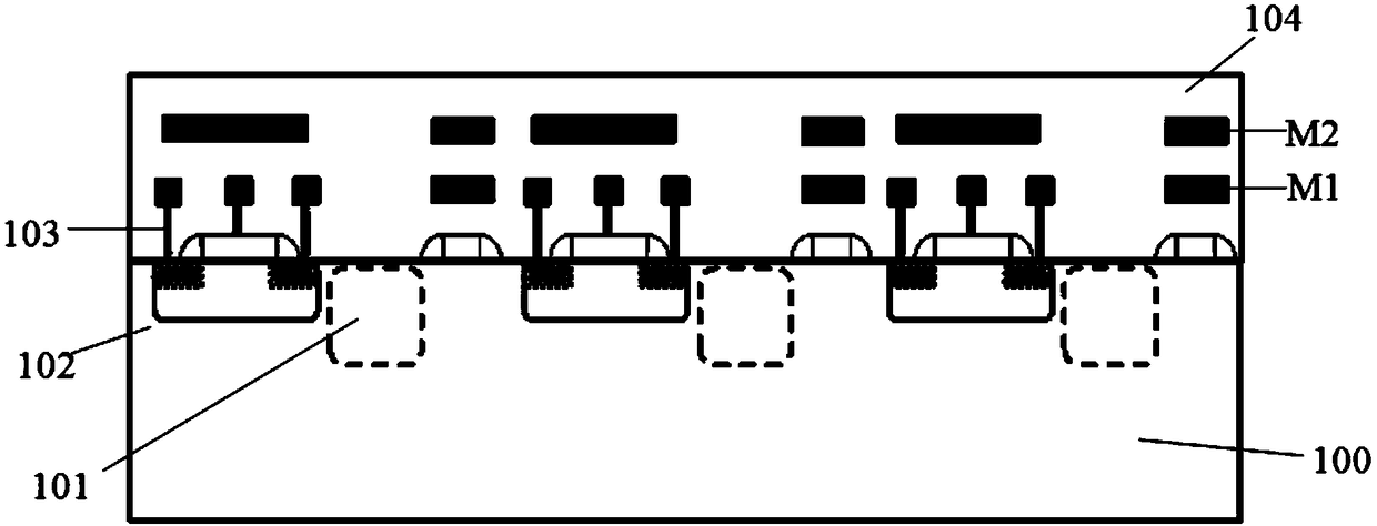
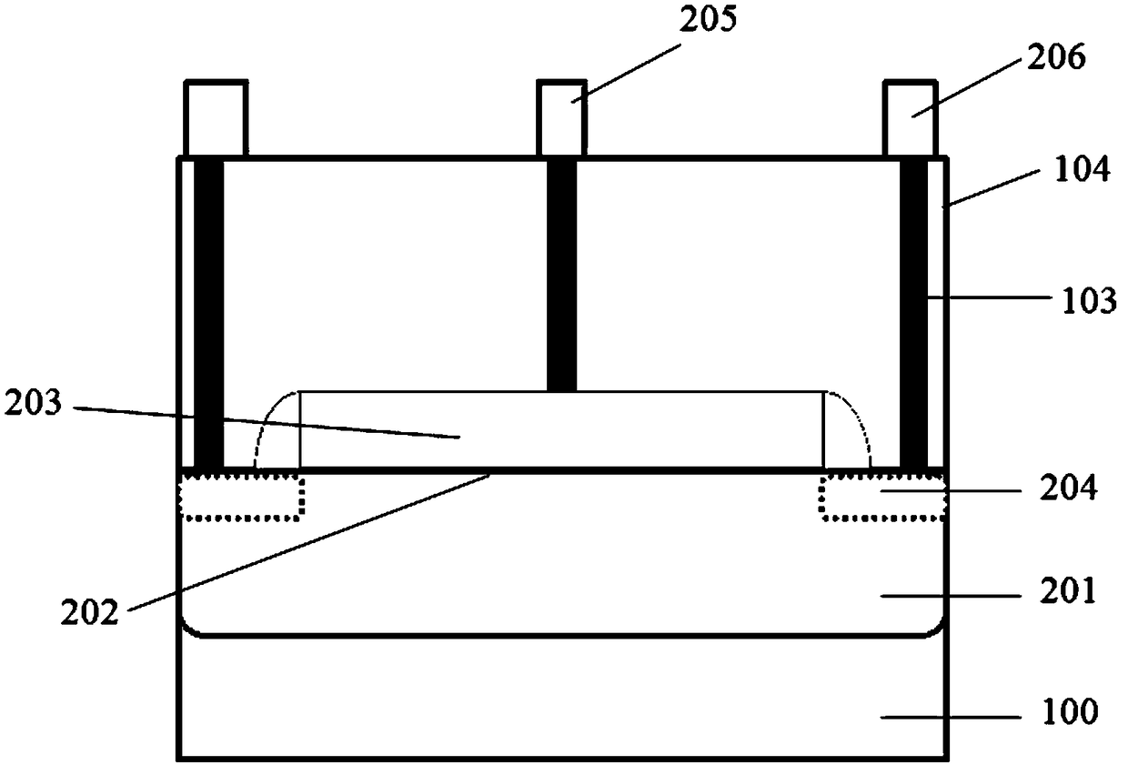
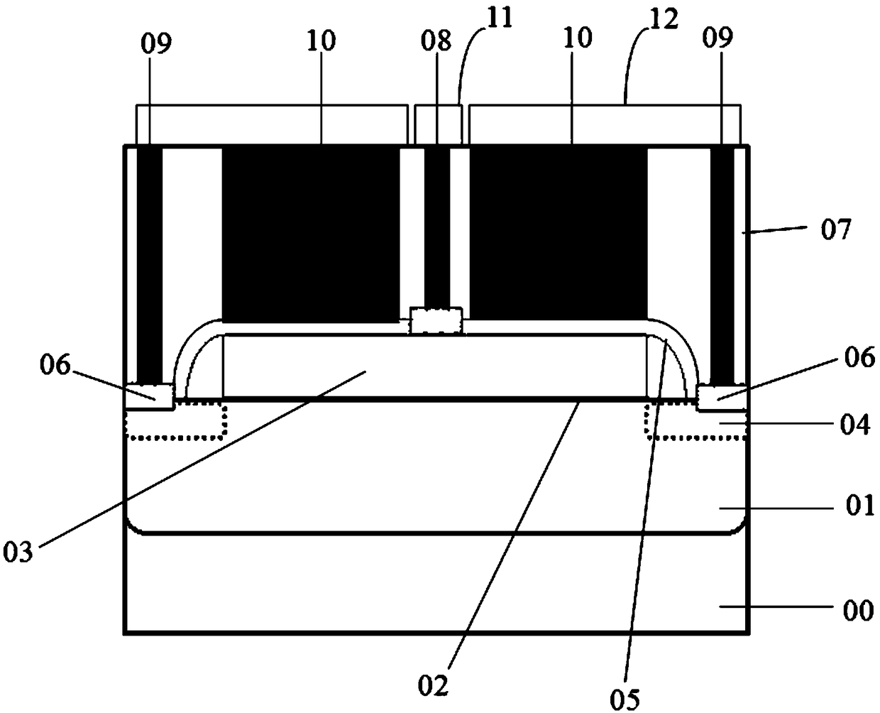
[0034] In the present invention, the capacitive structure of the global exposure pixel unit includes: a silicon substrate, a lower plate located on the silicon substrate, a first capacitive medium and an upper plate located on the lower plate in turn, and on both sides of the upper plate A source-drain region is provided on the surface of the lower plate, an interlayer dielectric is provided on the upper plate, the upper plate lead-out electrode is connected to the upper plate through a first contact hole, and the source-drain region is connected to the upper plate t...


PUM


Abstract

The invention provides a global exposure pixel unit, a capacitor structure and a preparation method. Through forming a first capacitor structure, a second capacitor structure and a third capacitor structure at a longitudinal direction, and connecting the three capacitor structures together in a parallel connection manner, on the basis of not increasing the area of the capacitor structure of the global exposure pixel unit, the storage capacitance value of the capacitor structure is increased, and the readout noise is reduced; and meanwhile, the area of a photodiode photosensitive area of the whole global exposure pixel unit is not affected, and the performance of a device is improved.

Description

technical field [0001] The invention relates to the field of semiconductor technology, in particular to a global exposure pixel unit, a capacitor structure and a preparation method thereof. Background technique [0002] An image sensor refers to a device that converts optical signals into electrical signals. Generally, large-scale commercial image sensor chips include charge-coupled device (CCD) and complementary metal-oxide semiconductor (CMOS) image sensor chips. [0003] Compared with traditional CCD sensors, CMOS image sensors have the characteristics of low power consumption, low cost and compatibility with CMOS technology, so they are more and more widely used. CMOS image sensors are now not only used in consumer electronics, such as miniature digital cameras (DSC), mobile phone cameras, video cameras and digital single-lens reflex (DSLR), but also in automotive electronics, monitoring, biotechnology and medical fields. . [0004] The pixel unit of the CMOS image sen...

Claims


Application Information

Patent Timeline
Patent Type & Authority Patents(China)
IPC IPC(8): H01L27/146
CPCH01L27/14603H01L27/14683
Inventor 顾学强范春晖奚鹏程
Owner SHANGHAI INTEGRATED CIRCUIT RES & DEV CENT
Why Eureka
Try Eureka