DRAM device and manufacturing method thereof

A device and storage device technology, applied in the field of DRAM devices and their formation, can solve the problems of poor compatibility, cost, complicated production process of eDRAM devices, etc., and achieve the effect of reducing the difficulty of production

Active Publication Date: 2016-04-27
SEMICON MFG INT (SHANGHAI) CORP
View PDF3 Cites 4 Cited by
  • Summary
  • Abstract
  • Description
  • Claims
  • Application Information

AI Technical Summary

Problems solved by technology

[0003] However, due to the complicated production process of eDRAM devices and poor compatibility with the production process of existing conventional semiconductor devices, it takes a lot of manpower and material resources to manufacture such devices

Method used


Image

  • DRAM device and manufacturing method thereof
  • DRAM device and manufacturing method thereof
  • DRAM device and manufacturing method thereof

Examples


Embodiment Construction

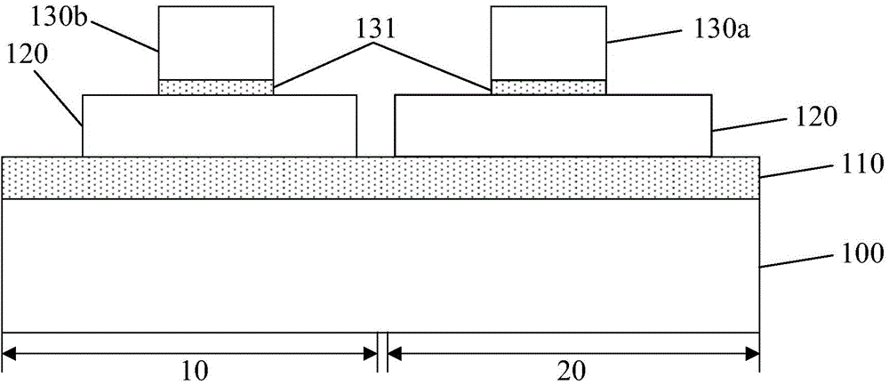
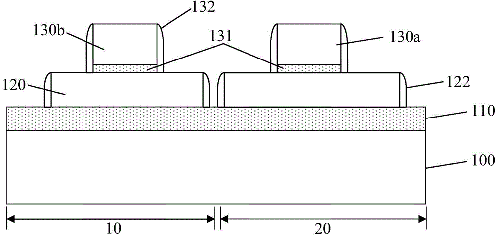
[0054] The process of making eDRAM devices in the prior art is cumbersome, one of the reasons is that the eDRAM devices need to add a capacitor structure in the transistor, and the method used in the prior art is to etch a substrate to form a deep trench (deeptrench ), and then sequentially form a semiconductor layer, a dielectric layer, and a semiconductor layer in the deep trench, so that the semiconductor layer, dielectric layer, and semiconductor layer form the capacitor; after the capacitor is formed, the logic part of the eDRAM device is formed And storage parts, such as gate, source and drain. However, this method is quite different from the current conventional process for manufacturing semiconductors, because the conventional process is generally carried out according to the main steps of substrate-gate-source-drain. After the bottom step, an additional process of forming a capacitor is added, that is to say, the existing process of forming an eDRAM device is not comp...


PUM

PropertyMeasurementUnit
Thicknessaaaaaaaaaa

Abstract

The invention provides a DRAM device and a manufacturing method thereof. The manufacturing method of the DRAM device comprises steps that, a substrate is provided; a first grid electrode and a second grid electrode are formed; source electrodes or drain electrodes of a logic transistor and a channel transistor are formed, a dielectric layer and a metal layer are formed, and the dielectric layer and the source electrode or the drain electrode of the channel transistor commonly form a capacitor. The DRAM device comprises the substrate, the channel transistor, the capacitor and the logic transistor, wherein the dielectric layer and the metal layer are sequentially arranged on the source electrode or the drain electrode of the transistor, and the source electrode or the drain electrode, the dielectric layer and the metal layer are used for forming the capacitor. The method and the device are advantaged in that, the dielectric layer and the metal layer are formed on the source electrode or the drain electrode of the channel transistor for forming the capacitor, a problem that a special deep trench for forming a capacitor is formed in a substrate in the prior art can be solved, the manufacturing process is simplified, manufacturing complexity is reduced, and compatibility with the routine manufacturing flow can be better.

Description

technical field [0001] The invention relates to the field of semiconductor manufacturing, in particular to a DRAM device and a forming method thereof. Background technique [0002] With the continuous development of the semiconductor industry, semiconductor devices with storage functions occupy an increasingly important position. Taking dynamic random access memory (Dynamic Random Access Memory, DRAM) as an example, embedded DRAM (embedded DRAM, eDRAM) in the DRAM category has been gradually applied to the market because of its higher operating speed and integration. [0003] However, since the production process of eDRAM devices is relatively complicated and is poorly compatible with the production process of existing conventional semiconductor devices, it requires a lot of manpower and material resources to manufacture such devices. On the other hand, even if the performance of the eDRAM device is improved compared with the traditional storage device, with the development...

Claims


Application Information

Patent Timeline
IPC IPC(8): H01L27/108H01L21/8242
Inventor 肖德元
Owner SEMICON MFG INT (SHANGHAI) CORP
Why Eureka
Try Eureka