esd device, manufacturing method of esd device and eeprom

An ESD device and manufacturing method technology, applied in semiconductor devices, electrical solid devices, electrical components, etc., can solve the problem of not meeting the needs of EEPRPM electrostatic protection capability, high turn-on voltage, unable to meet the electrostatic protection capability of semiconductor integrated circuits, etc.

Active Publication Date: 2019-04-09
SEMICON MFG INT (SHANGHAI) CORP
View PDF3 Cites 0 Cited by
  • Summary
  • Abstract
  • Description
  • Claims
  • Application Information

AI Technical Summary

Problems solved by technology

[0005] However, the turn-on voltage of the above-mentioned ESD device (referring to the absolute value of turn-on voltage here) is relatively high, so that it cannot meet the needs of semiconductor integrated circuits for electrostatic protection.
For example, HV 5V PMOS devices are usually used as ESD devices in existing EEPRPMs, and the turn-on voltage of HV 5V PMOS devices is usually -13V, while the design turn-on voltage of EEPRPM is -10V, which can no longer meet the needs of EEPRPM for electrostatic protection capabilities

Method used


Image

  • esd device, manufacturing method of esd device and eeprom
  • esd device, manufacturing method of esd device and eeprom
  • esd device, manufacturing method of esd device and eeprom

Examples


Embodiment Construction

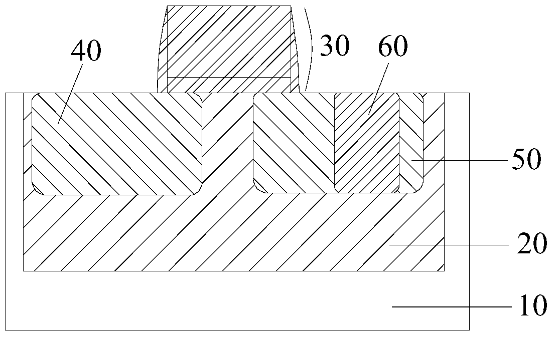
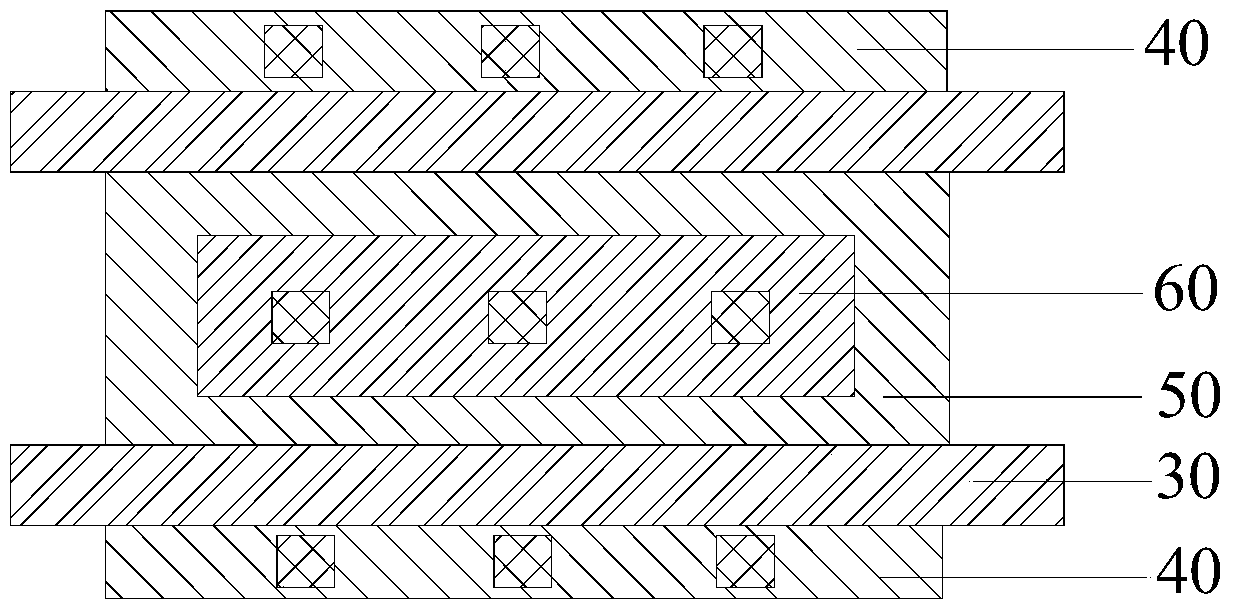
[0024] It should be noted that, in the case of no conflict, the embodiments in the present application and the features in the embodiments can be combined with each other. The present application will be described in detail below with reference to the accompanying drawings and embodiments.

[0025] It should be noted that the terminology used here is only for describing specific implementations, and is not intended to limit the exemplary implementations according to the present application. As used herein, unless the context clearly dictates otherwise, the singular is intended to include the plural, and it should also be understood that when the terms "comprising" and / or "comprising" are used in this specification, they mean There are features, steps, operations, means, components and / or combinations thereof.

[0026] For the convenience of description, spatially relative terms may be used here, such as "on ...", "over ...", "on the surface of ...", "above", etc., to describe...


PUM


Abstract

The invention discloses an ESD device, a manufacturing method of the ESD device and an EEPROM. The ESD device comprises a semiconductor base body, a trap arranged in the semiconductor base body, a grid electrode structure arranged on the surface of the trap, a source electrode, a drain electrode and an ion injection region. The source electrode is arranged in the trap and on one side of the grid electrode structure. The drain electrode is arranged in the trap and on the other side of the grid electrode structure. The conduction types of the source electrode and of the drain electrode are opposite to the conduction type of the trap. The ion injection region is arranged in the drain electrode. The conduction type of the ion injection region is opposite to that of the drain electrode. Via the ion injection region, the doping density in the drain electrode can be reduced, so probability of impact ionization of charge carriers and neutral atoms between the drain electrode and the semiconductor base body is increased, thereby reducing backward voltage required by avalanche breakdown between the drain electrode and the semiconductor base body, and further reducing starting voltage of the ESD device.

Description

technical field [0001] The present application relates to the technical field of semiconductor integrated circuits, and in particular, relates to an ESD device, a manufacturing method of the ESD device, and an EEPROM. Background technique [0002] The entire life cycle of semiconductor integrated circuits from growth to packaging and testing will face various unpredictable electrostatic environments, which will easily introduce static electricity into semiconductor integrated circuits, which will cause electrostatic damage to semiconductor integrated circuits. Therefore, the design of semiconductor integrated circuits not only needs to meet functional requirements, but also has a certain electrostatic protection capability. Especially for EEPROM (Electrically Erasable Programmable Read-Only Memory), since the EEPROM contains many high-voltage devices, it needs to have a certain electrostatic protection capability. [0003] At present, ESD devices are usually designed in sem...

Claims


Application Information

Patent Timeline
Patent Type & Authority Patents(China)
IPC IPC(8): H01L27/02H01L27/115
Inventor 王孝远郭兵金凤吉马燕春
Owner SEMICON MFG INT (SHANGHAI) CORP
Why Eureka
Try Eureka