A two-dimensional photonic crystal electromagnetic radiation protection device with isi structure
A technology of electromagnetic radiation protection and two-dimensional photonic crystals, which is applied in the direction of electrical components and interference to communication, etc., can solve problems such as inability to deform, not considering material thickness and coverage, and influence on emission efficiency
- Summary
- Abstract
- Description
- Claims
- Application Information
AI Technical Summary
Problems solved by technology
Method used
Image
Examples
Embodiment 1
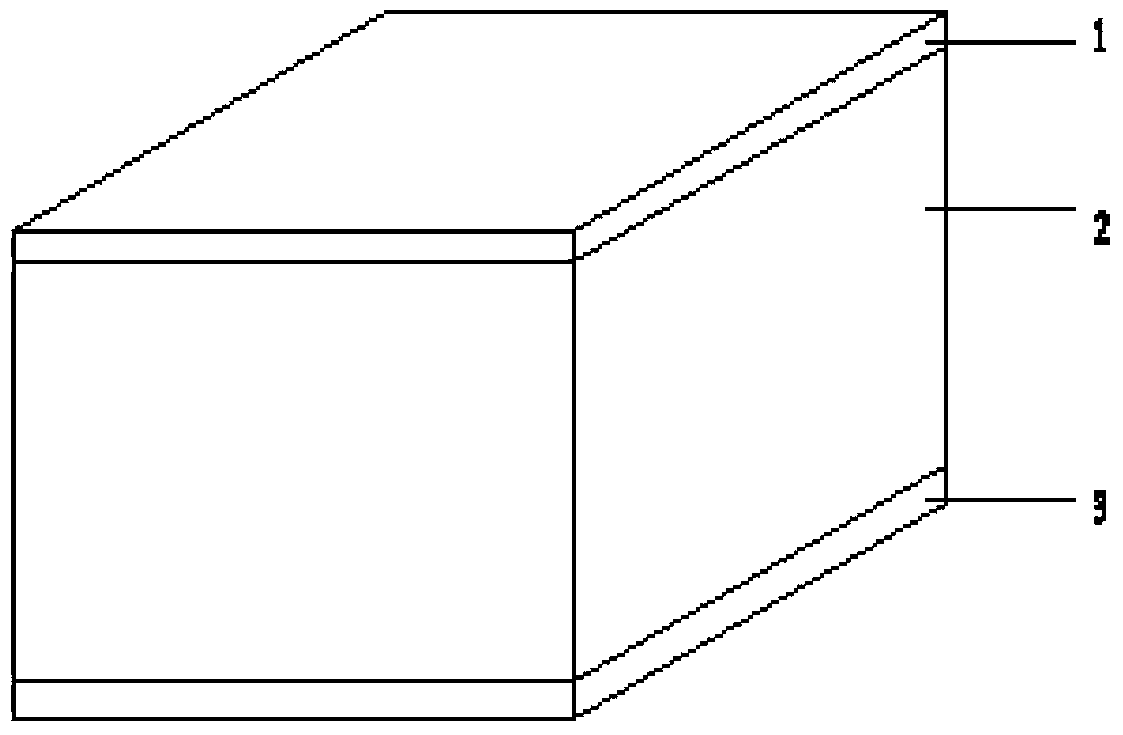
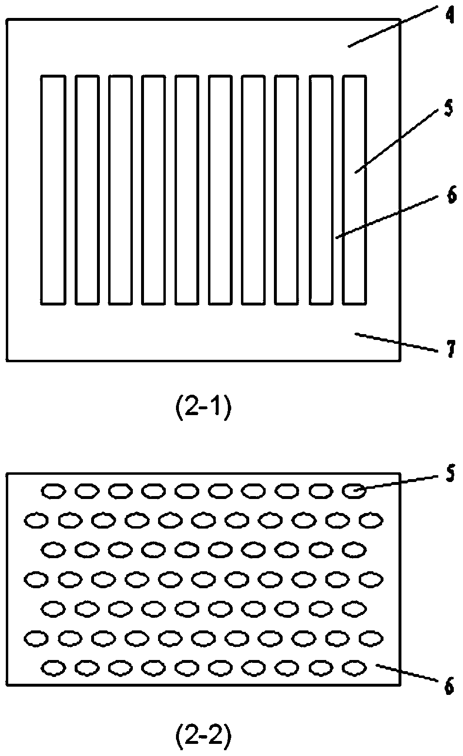
[0044] The ISI overall structure 2 described in this embodiment adopts a single-layer ISI photonic crystal structure to realize a larger forbidden band in the TE mode, and its overall structure is as follows figure 1 As shown, it includes a camouflage paint or camouflage clothing layer 1, an ISI overall structure 2 and an adhesion layer 3; the single-layer ISI photonic crystal structure 2 is composed of an upper insulator 4, a semiconductor dielectric column 5, an intermediate insulator 6 and a bottom insulator 7. The upper insulator 4, the intermediate insulator 6 and the bottom insulator 7 are all made of soft plastic with a refractive index of 1.45, and the semiconductor dielectric column 5 is used with a refractive index of 3.50 for the intrinsic semiconductor silicon; the silicon scattering elements are elliptical, and the spatial arrangement is triangular Lattice structure; in order to ensure the effect of the forbidden band, the minimum cutting unit of this structure sho...
Embodiment 2
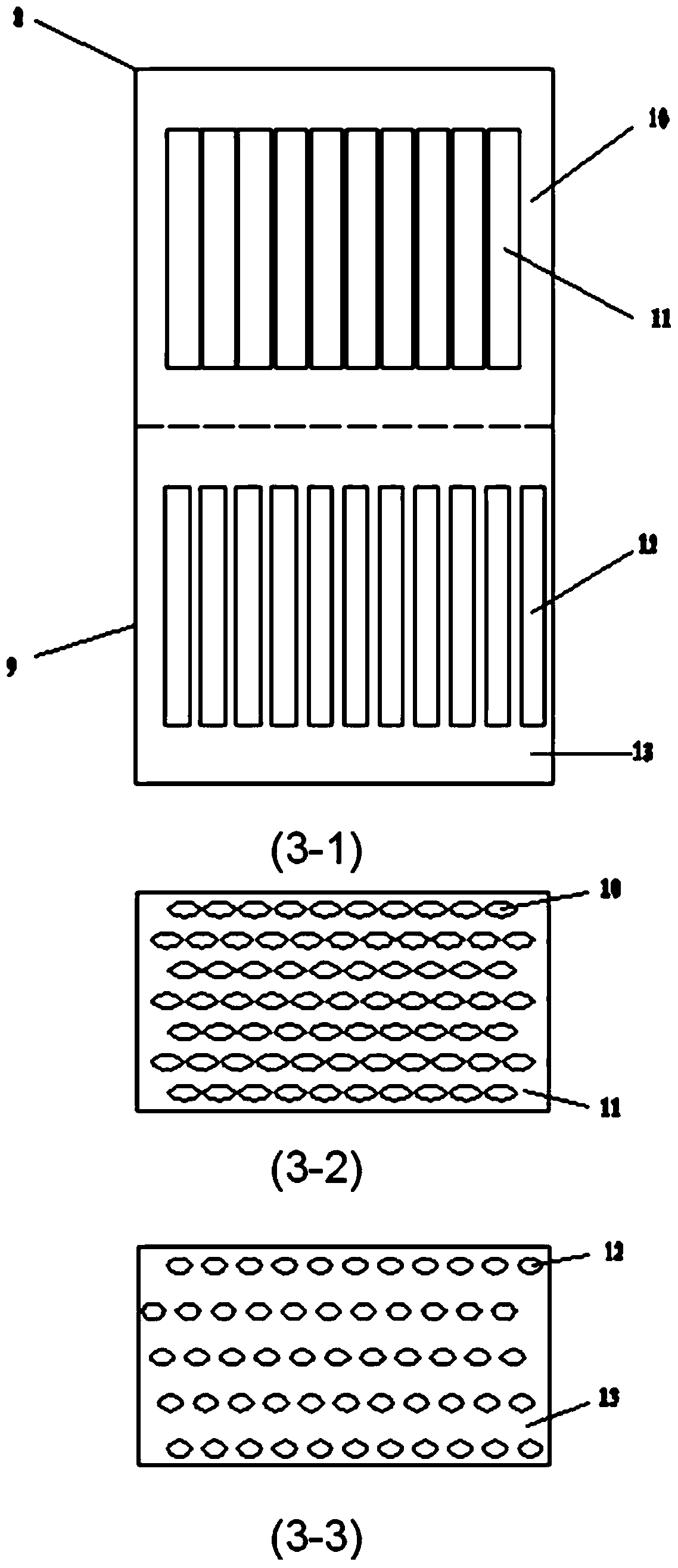
[0048] The ISI overall structure 2 described in this embodiment adopts a double-layer ISI photonic crystal structure to realize that both the TE mode and the TM mode have larger forbidden bands, and its overall structure is as follows figure 1 As shown, it includes camouflage paint or camouflage clothing layer 1, ISI overall structure 2 and adhesion layer 3. However, the overall structure 2 of the ISI structure is composed of two single-layer ISI photonic crystal structures connected in series, such as image 3 As shown, (3-1) is a side sectional view; (3-2) is a planar view of the upper part; (3-3) is a planar view of the lower part; wherein, the upper layer ISI photonic crystal structure 8 includes an upper layer semiconductor dielectric column 10 and an upper insulator 11; the lower ISI photonic crystal structure 9 includes a lower semiconductor dielectric column 12 and a lower insulator 13. The upper layer semiconductor dielectric column 10 and the lower layer semiconduct...
PUM
 Abstract
Description
Claims
Application Information
 - R&D
- Intellectual Property
- Life Sciences
- Materials
- Tech Scout
- Unparalleled Data Quality
- Higher Quality Content
- 60% Fewer Hallucinations
Browse by: Latest US Patents, China's latest patents, Technical Efficacy Thesaurus, Application Domain, Technology Topic, Popular Technical Reports.
© 2025 PatSnap. All rights reserved.Legal|Privacy policy|Modern Slavery Act Transparency Statement|Sitemap|About US| Contact US: help@patsnap.com


