Electromagnetic shielding package assembly and manufacturing method thereof

A manufacturing method and electromagnetic shielding technology, applied in semiconductor/solid-state device manufacturing, electrical components, electric solid-state devices, etc., can solve problems such as unfavorable electromagnetic shielding effect, electrical connection, and failure to obtain, and achieve the effect of improving electromagnetic shielding characteristics

Active Publication Date: 2018-08-03
HEFEI SMAT TECH CO LTD
View PDF8 Cites 0 Cited by
  • Summary
  • Abstract
  • Description
  • Claims
  • Application Information

AI Technical Summary

Problems solved by technology

However, in this electromagnetic shielding packaging group of the prior art, since the electromagnetic shielding cover is exposed outside the plastic package, the electromagnetic shielding cover will be affected by unfavorable factors such as ambient temperature and water vapor, which is not conducive to the electromagnetic shielding effect. In addition, due to the electromagnetic shielding The shielding cover is all exposed, so it cannot be electrically connected to the external circuit, for example, it cannot be electrically connected to the ground terminal, so that a higher electromagnetic shielding effect cannot be obtained

Method used


Image

  • Electromagnetic shielding package assembly and manufacturing method thereof
  • Electromagnetic shielding package assembly and manufacturing method thereof
  • Electromagnetic shielding package assembly and manufacturing method thereof

Examples


Embodiment Construction

[0042] Hereinafter, the present invention will be described in more detail with reference to the accompanying drawings. In the various drawings, the same components are denoted by similar reference numerals. For the sake of clarity, various parts in the drawings have not been drawn to scale. Also, some well-known parts may not be shown. For simplicity, the structure obtained after several steps can be described in one figure. In the following, many specific details of the present invention are described, such as the structure, material, size, process and technique of each constituent part, for a clearer understanding of the present invention. However, the invention may be practiced without these specific details, as will be understood by those skilled in the art.

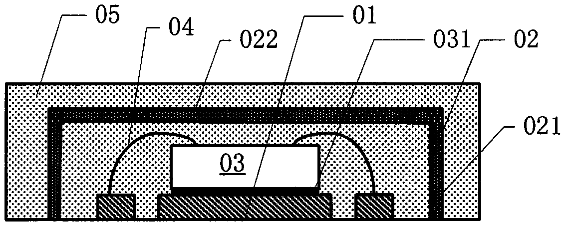
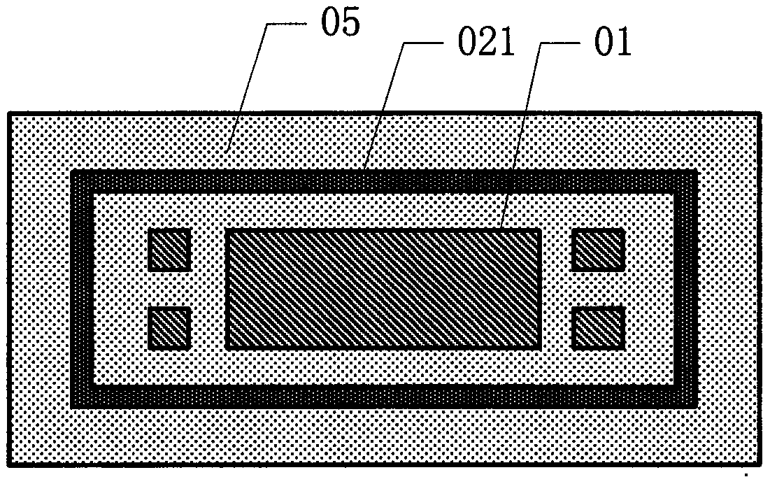
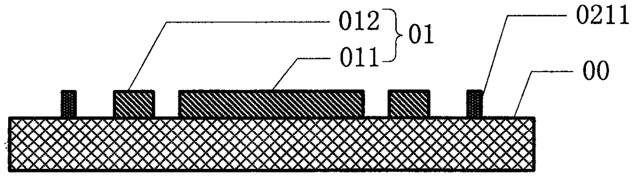
[0043] figure 1 It is a schematic cross-sectional structure diagram of an electromagnetic shielding package assembly according to an embodiment of the present invention. figure 2 for figure 1 Bottom view of t...


PUM


Abstract

The invention provides an electromagnetic shielding packaging component and a manufacturing method thereof, which belong to the field of semiconductor device packaging. An electromagnetic shielding cover is formed inside the electromagnetic shielding package assembly, and the bottom of the side wall of the electromagnetic shielding cover and the chip carrier are exposed on the surface of the plastic package as an electrode terminal electrically connected to an external circuit, which effectively improves the Electromagnetic shielding characteristics of electromagnetic shielding package components.

Description

technical field [0001] The invention relates to the technical field of semiconductor device packaging, in particular to an electromagnetic shielding packaging component and a manufacturing method thereof. Background technique [0002] At present, with the trend of multi-functionalization and miniaturization of electronic products, high-density microelectronic assembly technology has gradually become the mainstream in the new generation of electronic products, especially in hand-held portable products. The sudden increase in micro-assembly density and integration has put forward higher requirements for electromagnetic shielding of devices with strong electromagnetic radiation in a limited space, and the process difficulty has increased. [0003] In the existing electromagnetic shielding packaging components, after the plastic package of the packaging component is formed by the plastic packaging process, an electromagnetic shielding cover is formed on the surface of the plasti...

Claims


Application Information

Patent Timeline
Patent Type & Authority Patents(China)
IPC IPC(8): H01L23/552H01L23/31H01L21/56
CPCH01L2224/32245H01L2224/48247H01L2224/73265H01L2224/83005H01L2224/85005H01L2924/181H01L2924/3025H01L2924/00012H01L2924/00
Inventor 尤文胜
Owner HEFEI SMAT TECH CO LTD
Why Eureka
Try Eureka