A bidirectional absorber structure for visible light
A technology of absorber and visible light, which is applied in the direction of microstructure technology, microstructure device, manufacturing microstructure device, etc., can solve the inherent limitation of the absorption efficiency of light absorber, the inability of visible light absorber junction to achieve perfect absorption of two-way incident light at the same time, Solve problems such as waste of light energy, achieve the effect of bidirectional visible light absorption, simple structure, and low material consumption
- Summary
- Abstract
- Description
- Claims
- Application Information
AI Technical Summary
Problems solved by technology
Method used
Image


Examples
Embodiment 1
[0024] The manufacturing process of a visible light two-way absorber in this embodiment is as follows:
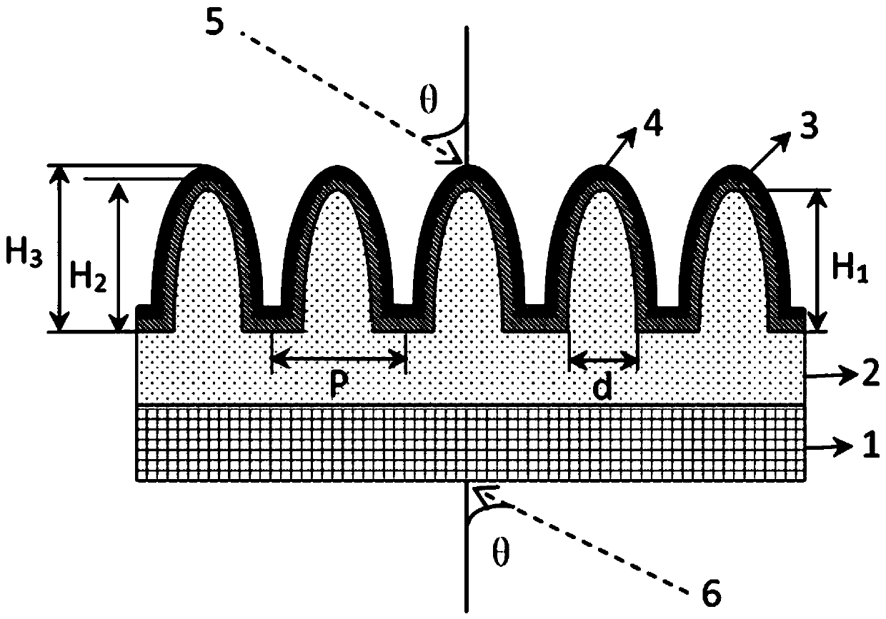
[0025] (1) Using polyethylene terephthalate as the base material, using the well-known technology in this field that we reported earlier - soft nanoimprint technology (Advanced Functional Materials, 25(18), 2660-2668), in Preparation of nanostructure units made of UV-curable adhesive on the substrate (such as figure 2 shown), the nanostructure unit period is P = 180 nm, and the height is H 1 =300 nm, the bottom width is d=65 nm;
[0026] (2) A layer of metal Au was evaporated on the above-mentioned nanostructure unit by thermal evaporation method, with a thickness (H 3 -H 2 ) =20nm;
[0027] (3) The dielectric layer silicon nitride film (SiN) was fabricated on the metal layer Au by magnetron sputtering 3 N 4 ), thickness (H 3 -H 2 )=18nm.
[0028] Ultimately, as Figure 3a As shown, the forward average absorptivity of the obtained visible two-way absorber device ...
Embodiment 2
[0030] The manufacturing process of a visible light two-way absorber in this embodiment is as follows:
[0031] (1) The preparation of the nanostructure unit is the same as the step (1) in Example 1;
[0032] (2) A layer of metal Ni was prepared on the above-mentioned nanostructure unit by measuring and controlling sputtering method, the thickness (H 3 -H 2 )=15nm;
[0033] (3) Using the magnetron sputtering method to make a dielectric layer silicon nitride film (Si 3 N 4 ) thickness (H 3 -H 2)=10nm.
[0034] The result is as Figure 6 As shown, the obtained visible two-way absorber device has a forward average absorption rate of 89.1% in the entire 300 nm-800 nm visible light band, and a corresponding reverse average absorption rate of 67.4%.
Embodiment 3
[0036] The manufacturing process of a visible light two-way absorber in this embodiment is as follows:
[0037] (1) A single crystal silicon wafer was used as the substrate material, and nanostructure units were prepared on the single crystal silicon wafer by electron beam etching, with a period of P = 120 nm and a height of H 1 =250 nm, the bottom width is d=60 nm;
[0038] (2) A layer of metal Au was evaporated on the above-mentioned nanostructure unit by thermal evaporation method, with a thickness (H 3 -H 2 ) =15nm;
[0039] (3) The dielectric layer silicon dioxide (SiO2) is made on the metal layer Au by thermal evaporation method. 2 ), thickness (H 3 -H 2 )=22nm.
[0040] Test the forward and reverse absorption rate of the prepared device, the results are as follows Figure 7 As shown, the obtained visible two-way absorber device has a forward average absorption rate of 88.1% in the entire 300 nm-800 nm visible light band, and a corresponding reverse average absorp...
PUM
| Property | Measurement | Unit |
|---|---|---|
| thickness | aaaaa | aaaaa |
| height | aaaaa | aaaaa |
| width | aaaaa | aaaaa |
Abstract
Description
Claims
Application Information
 - Generate Ideas
- Intellectual Property
- Life Sciences
- Materials
- Tech Scout
- Unparalleled Data Quality
- Higher Quality Content
- 60% Fewer Hallucinations
Browse by: Latest US Patents, China's latest patents, Technical Efficacy Thesaurus, Application Domain, Technology Topic, Popular Technical Reports.
© 2025 PatSnap. All rights reserved.Legal|Privacy policy|Modern Slavery Act Transparency Statement|Sitemap|About US| Contact US: help@patsnap.com