Common-ground high-gain Z source boost converter
A boost converter and high-gain technology, which is applied in the field of high-gain Z-source boost converters, can solve problems such as the inability to achieve a large amplitude, high stress on the switch tube, and different ground, and achieve simple structure, low stress, and high efficiency effect
- Summary
- Abstract
- Description
- Claims
- Application Information
AI Technical Summary
Problems solved by technology
Method used
Image
Examples
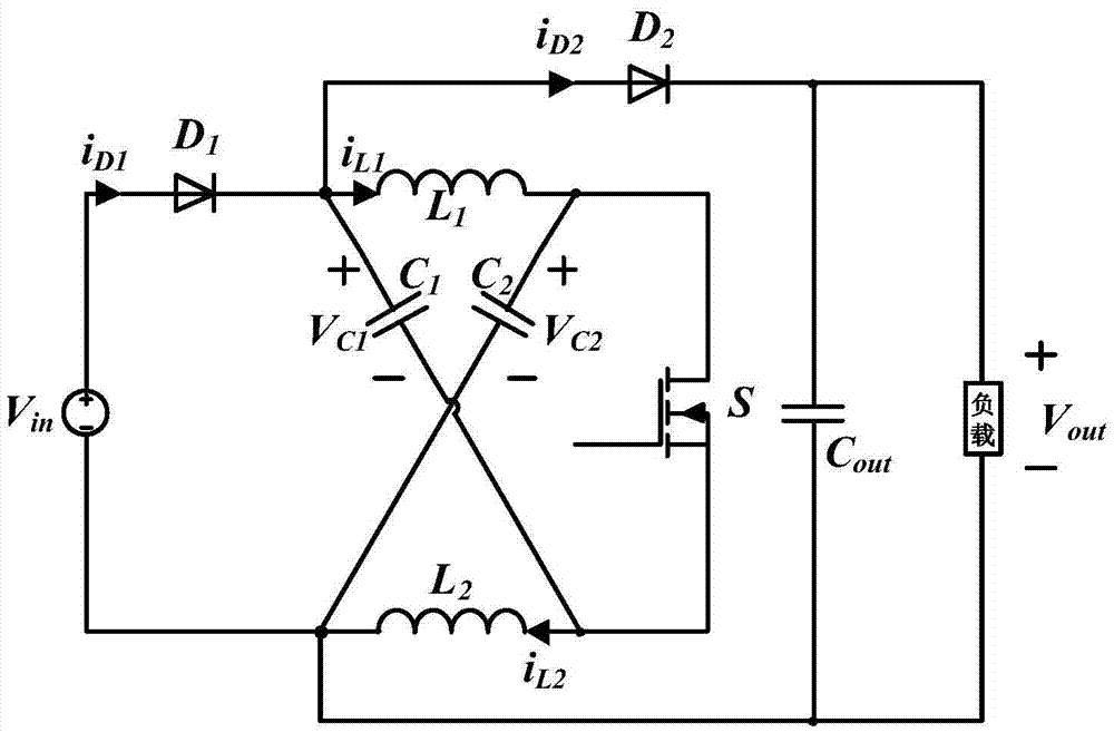
Embodiment Construction
[0011] In order to further illustrate the content and characteristics of the present invention, the specific embodiments of the present invention will be described below in conjunction with the accompanying drawings, but the implementation of the present invention is not limited thereto.
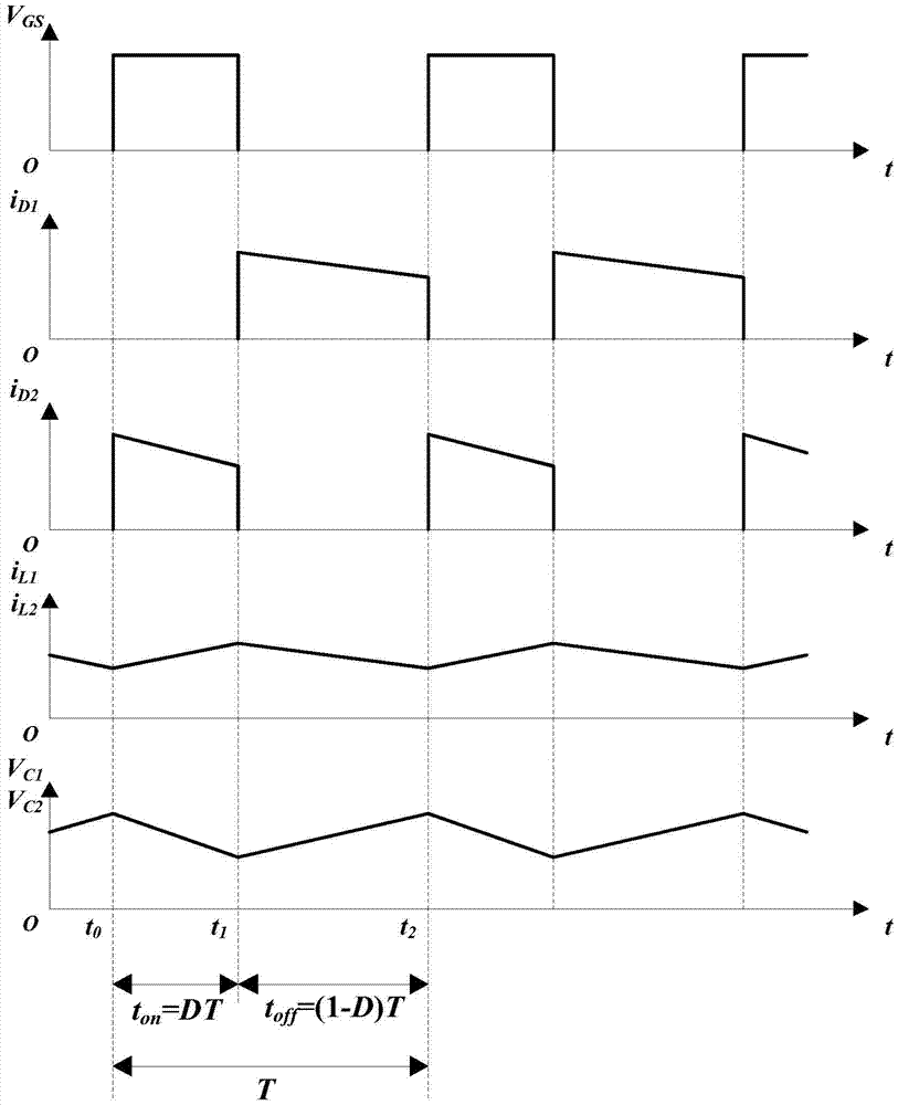
[0012] The basic topological structure of the present invention and the voltage and current reference direction of each main component are as follows: figure 1 shown. For the convenience of analysis, the devices in the circuit structure are regarded as ideal devices. The drive signal V of the switch tube S GS , the first diode D 1 current i D1 , the second diode D 2 current i D2 , the first inductance L 1 current i L1 , the second inductance L 2 current i L2 , the first capacitance C 1 Voltage V C1 , the second capacitance C 2 Voltage V C2 The wave form is as figure 2 shown.
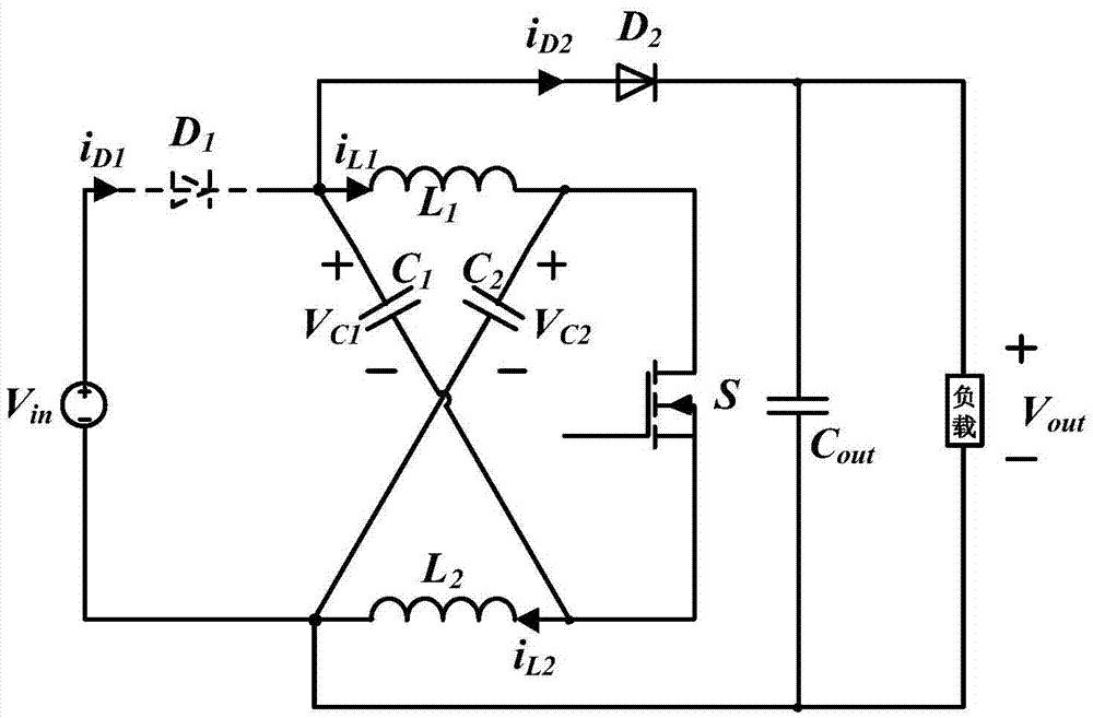
[0013] (1) at (t 0 ~t 1 ) stage, the modal diagram of the converter at this stage is as follows ...
PUM
 Abstract
Description
Claims
Application Information
 - R&D
- Intellectual Property
- Life Sciences
- Materials
- Tech Scout
- Unparalleled Data Quality
- Higher Quality Content
- 60% Fewer Hallucinations
Browse by: Latest US Patents, China's latest patents, Technical Efficacy Thesaurus, Application Domain, Technology Topic, Popular Technical Reports.
© 2025 PatSnap. All rights reserved.Legal|Privacy policy|Modern Slavery Act Transparency Statement|Sitemap|About US| Contact US: help@patsnap.com


