
Manufacturing method of gate oxide layer and manufacturing method of semiconductor device

A gate oxide layer and manufacturing method technology, applied in semiconductor/solid-state device manufacturing, semiconductor devices, electrical components, etc., can solve problems such as unreliable performance of field effect transistors, achieve dense gate oxide layer, and improve reliability Effect

Active Publication Date: 2018-11-16
SEMICON MFG INT (SHANGHAI) CORP
View PDF4 Cites 0 Cited by
  • Summary
  • Abstract
  • Description
  • Claims
  • Application Information

AI Technical Summary

Problems solved by technology

[0005] However, in the actual process, it is found that the performance of field effect transistors with gate oxide layers of different thicknesses fabricated by the above method is not reliable.

Method used


Image

  • Manufacturing method of gate oxide layer and manufacturing method of semiconductor device
  • Manufacturing method of gate oxide layer and manufacturing method of semiconductor device
  • Manufacturing method of gate oxide layer and manufacturing method of semiconductor device

Examples


Embodiment Construction

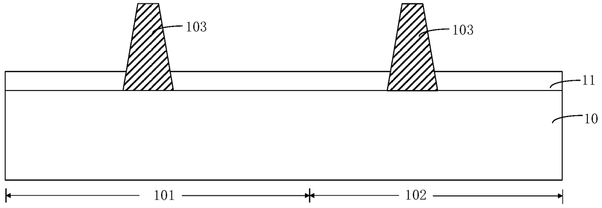
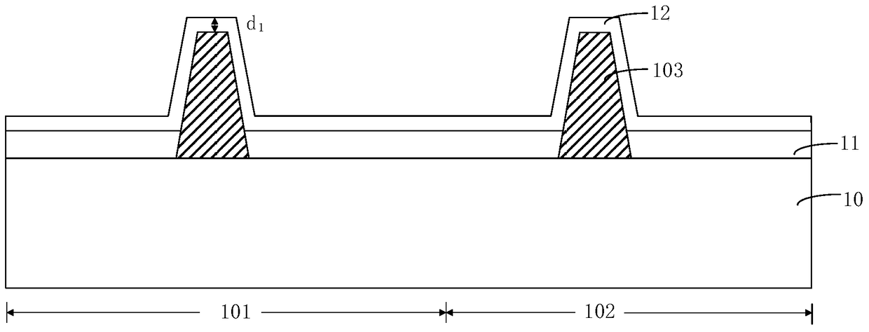
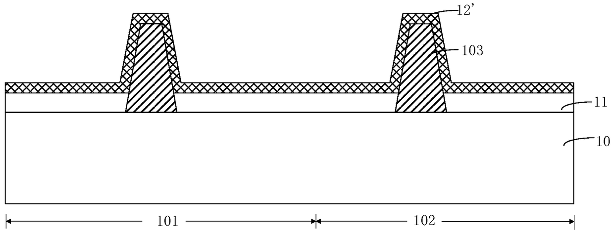
[0038] As mentioned in the background, existing field effect transistors perform unreliably. After analysis, the inventors found that there are more silicon dangling bonds in the gate oxide layer formed by the prior art, which causes the gate oxide layer to be relatively loose. The underlying channel region causes corrosion, which affects the performance of the field effect transistor formed. Based on the above analysis, the present invention uses a solution containing ozone to treat the gate oxide layer before photolithography, and the oxygen ions in the ozone can form bonds with the silicon dangling bonds in the gate oxide layer, that is, the oxygen ions in the ozone are used as filling Atoms fill the silicon dangling bonds of the gate oxide layer, making the gate oxide layer dense, preventing the developer from diffusing into it and causing corrosion to the channel region of the semiconductor substrate under the gate oxide layer, thereby improving the reliability of the fie...


PUM


Abstract

The invention discloses a grid oxidation layer manufacturing method and a semiconductor device manufacturing method. Ozone-containing solution is used for processing a grid oxidation layer before photoetching, and oxygen ions in ozone can be bonded with silicon dangling bonds in the grid oxidation layer. In other words, the oxygen ions in ozone serve as filling atoms which are used for filling the silicon dangling bonds in the grid oxidation layer, thereby enabling the grid oxidation layer to be compact, preventing the inward diffusion of developing solution from causing the corrosion of a trench region of a semiconductor substrate under the grid oxidation layer in a photoetching process, and improving the reliability of a field effect transistor.

Description

technical field [0001] The invention relates to the technical field of semiconductors, in particular to a method for manufacturing a gate oxide layer and a method for manufacturing a semiconductor device. Background technique [0002] Field Effect Transistors (FETs) are one of the most widely used semiconductor devices in integrated circuits. A typical field effect transistor includes: a semiconductor substrate, source and drain regions, and a gate structure. The gate structure includes a gate oxide layer and a gate. The source and drain regions are located on both sides of the channel, and the gate oxide layer separates the gate from the channel. [0003] One reason field-effect transistors can operate in a variety of ways is because the gate oxide layer has different thicknesses and can withstand different voltages. [0004] In the prior art, in order to fabricate field effect transistors with gate oxide layers of different thicknesses on the same semiconductor substrat...

Claims


Application Information

Patent Timeline
Patent Type & Authority Patents(China)
IPC IPC(8): H01L21/28H01L21/336
Inventor 刘佳磊
Owner SEMICON MFG INT (SHANGHAI) CORP
Learn More