
Touch-sensitive element and touch display device

A technology of touch sensing element and touch display device, which is applied in the direction of instrument, electrical digital data processing, input/output process of data processing, etc. The pixel aperture ratio of the device can be improved to improve the image quality and visual effect, improve the aperture ratio and reduce the cost.

Active Publication Date: 2016-03-30
BOE TECH GRP CO LTD +1
View PDF6 Cites 4 Cited by
  • Summary
  • Abstract
  • Description
  • Claims
  • Application Information

AI Technical Summary

Problems solved by technology

However, a defect caused by the setting of these touch signal lines is that it may affect the aperture ratio of the pixels of the display device, thereby affecting the image quality and visual effect of the final display product.
At the same time, in the actual manufacturing process, the formation of the touch pattern metal (TPM) brings additional materials and processes to the display device, resulting in an increase in the cost of the display device

Method used


Image

  • Touch-sensitive element and touch display device
  • Touch-sensitive element and touch display device
  • Touch-sensitive element and touch display device

Examples


Embodiment 1

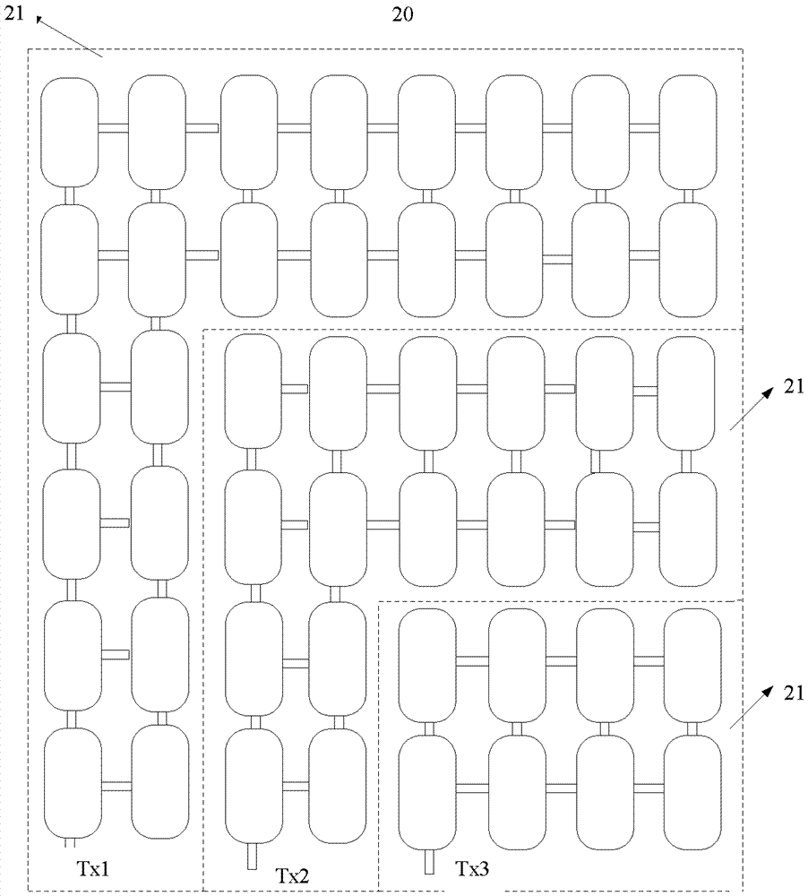
[0031] figure 2 The pattern of one touch sensing unit 10 in the touch sensing element according to one embodiment of the present invention is schematically shown, and it should be understood that the touch sensing element provided in this embodiment may include multiple such arrangements on the same layer of the touch sensing unit 10, in other words, figure 2 The touch sensing unit 10 shown in is just a repeating unit in the touch sensing element. In this embodiment, the touch-sensing element may include a plurality of touch-sensing units 10 arranged on the same layer, the touch-sensing unit 10 includes at least one first touch-sensing sub-unit 11, each first touch-sensing sub-unit 11 includes a first electrode The block array, the first electrode block array of the first touch sensing sub-unit 11 , is composed of a plurality of cascaded electrode blocks arranged on the same layer.

[0032] For clarity and simplicity, figure 2 Only three first touch sensing subunits 11 a...

Embodiment 2

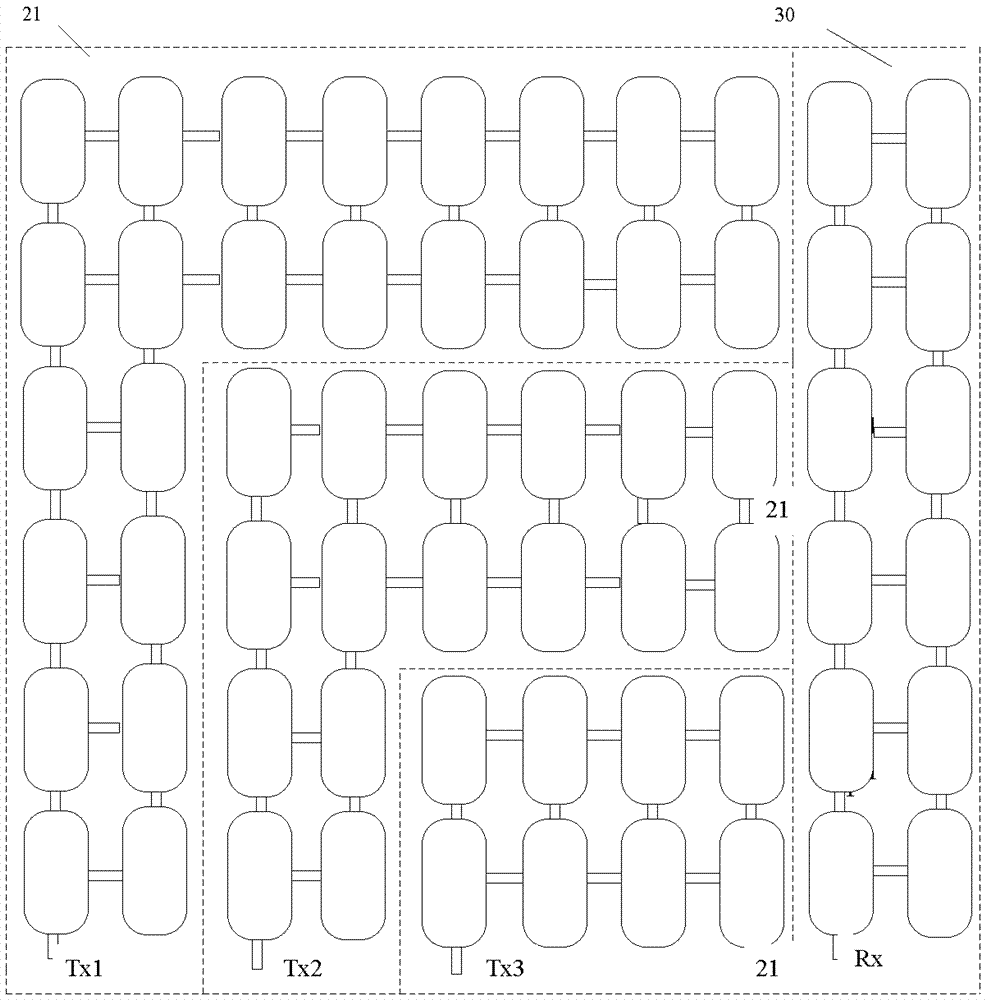
[0038] see Figure 5 , which schematically shows a touch sensing element according to another embodiment of the present invention. On the basis of Embodiment 1, a second touch sensing subunit 30 is added. The second touch sensing subunit includes a second electrode block array composed of a plurality of cascaded electrode blocks arranged on the same layer, and the second touch The sensing subunit is insulated from the first touch sensing subunit.

[0039] divide and figure 2 In addition to the same or similar structures, the structure of this embodiment with the addition of the second touch sensing sub-unit 30 can provide a structural basis for realizing mutual capacitive touch. Wherein each first touch sensing sub-unit 11 can be used as a drive electrode receiving drive signals Tx1, Tx2, Tx3 from the touch detection chip, and the second touch sensing sub-unit 30 can be used to provide sensing for the touch detection chip. Sensing electrode for signal Rx. As known to thos...


PUM


Abstract

The embodiment of the invention provides a touch-sensitive element and a touch display device. The touch-sensitive element comprises a plurality of touch-sensitive units, wherein each touch-sensitive unit comprises a plurality of first touch-sensitive subunits which at least can receive driving signals; each first touch-sensitive subunit comprises an electrode block array; and in the electrode block array of each first touch-sensitive subunit, any two adjacent electrode blocks are mutually connected in a line direction or row direction. The touch-sensitive element can be applied to the display device to realize touch control. Compared with the prior art, the touch-sensitive element omits TPM (Touch Pattern Metal), so that the aperture ratio of the pixel of the display device is improved so as to be favorable for improving the image quality and the visual effect of the display device, meanwhile, the manufacture technology of the TPM is omitted, and the cost of a touch panel or the display device can be lowered.

Description

technical field [0001] The present invention relates to the field of display technology, and more particularly to a touch sensing element and a touch display device. Background technique [0002] Many types of input devices are currently available for performing operations in computer systems, such as mice, buttons, touch screens, joysticks, and the like. However, due to the ease of use of touch screens, the versatility of operation, the declining price, and the steadily increasing yield rate, touch screens are becoming more and more popular. As touch screens gradually enter people's lives, the previous input devices have gradually been eliminated from people's field of vision. The touch screen can be divided into plug-in type and built-in type. The plug-in type touch screen is to position the panel with touch function in front of the display device, and the touch surface covers the visible area of ​​the display area. The built-in touch screen integrates the touch function...

Claims


Application Information

Patent Timeline
Patent Type & Authority Applications(China)
IPC IPC(8): G06F3/041
CPCG06F3/0416G06F3/0412G06F3/04164G06F3/04166G06F3/0443G06F3/047
Inventor 古宏刚邵贤杰宋洁刘承娜
Owner BOE TECH GRP CO LTD
Learn More