Light emitting diode package structure
A technology for light-emitting diodes and packaging structures, which is applied to electrical components, circuits, semiconductor devices, etc., can solve problems such as the quality degradation of light-emitting diode packaging structures, and achieve the effect of improving quality
- Summary
- Abstract
- Description
- Claims
- Application Information
AI Technical Summary
Problems solved by technology
Method used
Image
Examples
no. 1 example
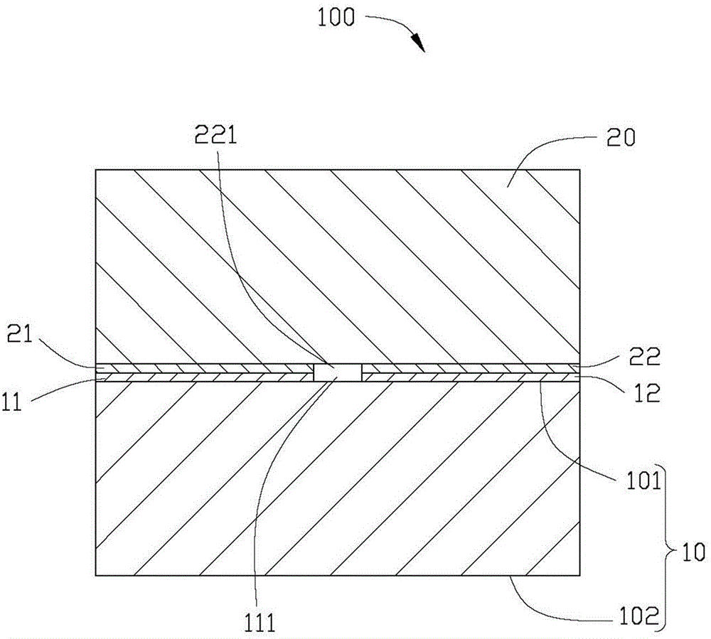
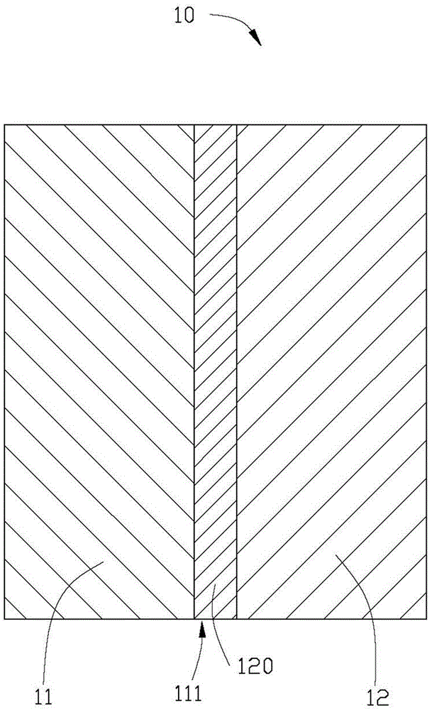
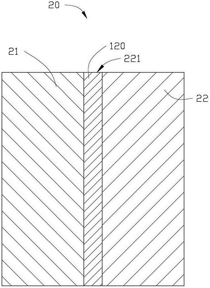
[0020] See figure 1 The light emitting diode packaging structure 100 of this embodiment includes a substrate 10 and a light emitting diode chip 20 disposed on the substrate 10, the first welding area 11 and the second welding area 12 are arranged at intervals on the substrate 10, the light emitting diode chip 20 includes a first electrode 21 and a second electrode 22 arranged at intervals, the first electrode 21 and the second electrode 22 are symmetrically arranged and have the same area, and the first electrode 21 and the second electrode 22 are respectively connected to the first welding The area 11 and the second welding area 12 correspond to welding.
[0021] The substrate 10 can be any board that can be designed for wiring on its surface or inside. In this embodiment, the substrate 10 may be a common printed circuit board, a flexible circuit board, a PLCC (Plastic Leaded Chip Carrier) or a ceramic substrate.
[0022] The substrate 10 includes a welding surface 101 and ...
no. 2 example
[0028] See Figure 4 In the LED packaging structure 100a in this embodiment, the LED chip 20a includes a first electrode 21a, a second electrode 22a, and a third electrode 23a, and the first electrode 21a and the third electrode 23a are symmetrically arranged on The two opposite sides of the second electrode 22a, and the area of the first electrode 21a is equal to the area of the third electrode 23a.
[0029] See Figure 6 , A first spacing groove 221a is formed between the first electrode 21a and the second electrode 22a. A second spacing groove 222a is formed between the second electrode 22a and the third electrode 23a. The first spacing groove 221 a and the second spacing groove 222 a may be filled with insulating material 120 .
[0030] Accordingly, see Figure 5 The welding surface 101a of the substrate 10a is provided with a first welding area 11a, a second welding area 12a and a third welding area 13a. The first welding area 11a, the second welding area 12a and...
no. 3 example
[0035] See Figure 8 , in this embodiment, the substrate 10a further includes a third spacer region 113a. The third spacer 113a penetrates along the middle of the first welding zone 11a, the second welding zone 12a and the third welding zone 13a so as to connect the first welding zone 11a, the second welding zone 12a and the third welding zone. Area 13a is divided equally.
[0036] See Figure 9 , correspondingly, the LED chip 20a further includes a third spacing groove 223a corresponding to the third spacing region 113a of the substrate 10a. The third spacing groove 223a penetrates along the middle of the first electrode 21a, the second electrode 22a and the third electrode 23a to bisect the first electrode 21a, the second electrode 22a and the third electrode 23a.
PUM
 Abstract
Description
Claims
Application Information
 - Generate Ideas
- Intellectual Property
- Life Sciences
- Materials
- Tech Scout
- Unparalleled Data Quality
- Higher Quality Content
- 60% Fewer Hallucinations
Browse by: Latest US Patents, China's latest patents, Technical Efficacy Thesaurus, Application Domain, Technology Topic, Popular Technical Reports.
© 2025 PatSnap. All rights reserved.Legal|Privacy policy|Modern Slavery Act Transparency Statement|Sitemap|About US| Contact US: help@patsnap.com


