Mesoscopic solar cell based on perovskite-kind light absorption material and preparation method thereof
A solar cell, perovskite technology, applied in the field of solar cells
- Summary
- Abstract
- Description
- Claims
- Application Information
AI Technical Summary
Problems solved by technology
Method used
Image
Examples
Embodiment 1
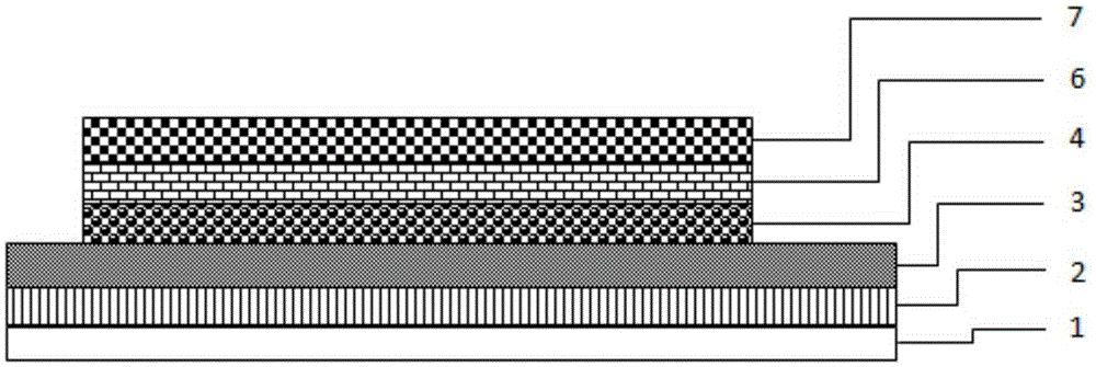
[0074] The device in this embodiment uses glass as the substrate 1, on which a transparent conductive glass 2 is arranged, and then after depositing a certain thickness such as a 50nm titanium dioxide hole blocking layer 3 thereon, it is sequentially screen-printed from bottom to top. Electron transport layer 4 (such as titanium dioxide), electron blocking layer 6 (preferably tungsten oxide) and back electrode layer 7 (preferably carbon material) are prepared.
[0075] In the electron transport layer 4 , the grain size of nano titanium dioxide is, for example, 18 nm, and the thickness of the titanium dioxide layer is, for example, about 1 μm. In the electron blocking layer 6 , the particle size of tungsten oxide is, for example, 30 nanometers, and the thickness is, for example, about 1 μm. The back electrode layer 7 is preferably a mesoporous conductive film made of graphite or carbon black, with a thickness of about 10 μm, for example. A certain amount, such as 40 μL perovsk...
Embodiment 2
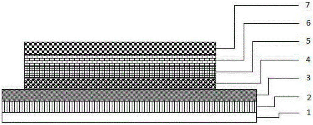
[0077] The device in this embodiment uses glass as the substrate 1, on which a transparent conductive glass 2 is arranged, and then after depositing a certain thickness such as a 50nm titanium dioxide hole blocking layer 3 thereon, it is sequentially screen-printed from bottom to top. Electron transport layer 4 (such as titanium dioxide), insulating spacer layer 5 (such as zirconium dioxide), electron blocking layer 6 (preferably tungsten oxide) and back electrode layer 7 (preferably aluminum material) are prepared.
[0078] In this embodiment, the grain size of nano titanium dioxide is, for example, 18 nm, and the thickness of the titanium dioxide electron transport layer 4 is, for example, about 1 μm. The grain size of zirconia is, for example, 40 nm, and the thickness of the insulating spacer layer is, for example, about 1 μm. The particle size of tungsten oxide in the electron blocking layer 6 is, for example, 30 nanometers, and the thickness is, for example, 100 nanometer...
Embodiment 3
[0082] The device in this embodiment uses glass as the substrate 1, on which a transparent conductive glass 2 is arranged, and a 30nm titanium dioxide dense layer 3, a titanium dioxide electron transport layer 4, and a tungsten oxide electron blocking layer are sequentially prepared by 3D printing from bottom to top 6. A certain amount, such as 100 μL perovskite (PEA) 2 (CH 3 NH 3 ) 40 Pb 41 Cl 10 I 114 (PEA stands for phenylethylamine, the same below) The precursor solution (40wt%) is spin-coated on the above-mentioned semiconductor layer, and left to stand for one minute until it fully penetrates into the titanium dioxide nanocrystalline film, and then dried at a certain temperature such as 50°C. A carbon back electrode layer 7 is printed. The test shows that the obtained battery device is at 100mW / cm 2 The efficiency under simulated sunlight is 20.5%.
PUM
| Property | Measurement | Unit |
|---|---|---|
| Thickness | aaaaa | aaaaa |
| Diameter | aaaaa | aaaaa |
| Thickness | aaaaa | aaaaa |
Abstract
Description
Claims
Application Information
 - R&D
- Intellectual Property
- Life Sciences
- Materials
- Tech Scout
- Unparalleled Data Quality
- Higher Quality Content
- 60% Fewer Hallucinations
Browse by: Latest US Patents, China's latest patents, Technical Efficacy Thesaurus, Application Domain, Technology Topic, Popular Technical Reports.
© 2025 PatSnap. All rights reserved.Legal|Privacy policy|Modern Slavery Act Transparency Statement|Sitemap|About US| Contact US: help@patsnap.com


