
membrane switch

A membrane switch and base material technology, applied in the electronic field, can solve problems such as high defect rate of lines, many production processes, and poor waterproof ability, and achieve the effects of reducing production processes, simple production processes, and low cost

Active Publication Date: 2018-02-27
JIANGSU TRANSIMAGE TECH CO LTD
View PDF5 Cites 0 Cited by
  • Summary
  • Abstract
  • Description
  • Claims
  • Application Information

AI Technical Summary

Problems solved by technology

[0002] The existing membrane switch adopts a three-layer structure, including an upper circuit board, an insulating layer and a lower circuit board, wherein the upper circuit board and the lower circuit board include a base material and a printed silver wire circuit, the upper circuit board and the insulating layer, the insulating layer and the The lower circuit boards are bonded by glue. The production process includes printing silver wires on the upper layer and the lower layer, jumper wires, and gluing. There are many production processes and high costs. When printing silver wires, the defective rate of the circuit is very high, and the waterproof ability is relatively low. Difference
[0003] Moreover, the above-mentioned circuit board mostly uses polyimide film as the base material, and its cost is also very high.

Method used


Image

  • membrane switch
  • membrane switch
  • membrane switch

Examples


Embodiment Construction

[0024] The technical solution of the present invention will be further described below in conjunction with the accompanying drawings.

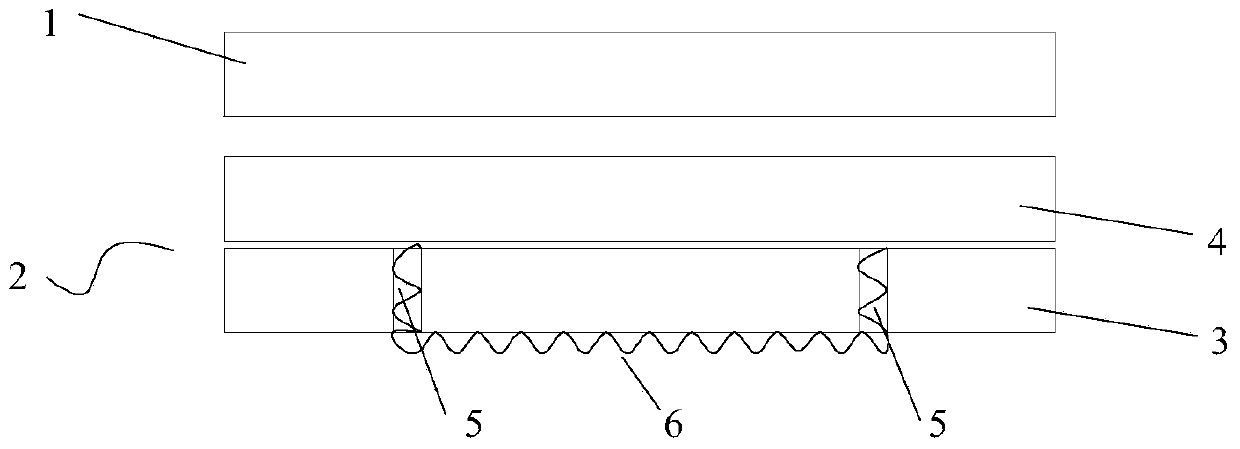
[0025] Such as figure 1 As shown, the membrane switch of the present invention includes an upper conductive circuit 1, a lower conductive circuit 2 and an insulating part between them, the lower conductive circuit 2 includes a base material 3 and an etched metal circuit 4 located above the base material 3, the The base material 3 is provided with at least one pair of through holes 5, and the inside of the through holes 5 and the bottom of the base material between the two through holes 5 are provided with a conductive coating 6, so that the base material 3 and the etched metal circuit 4 form a conductive closure. circuit, conduction direction as figure 2 .

[0026] The substrate 3 can be a polyimide film, a polyester film, a polycarbonate film, a polyvinyl chloride film or other flexible substrates, preferably a polyester film, and the poly...


PUM


Abstract

The invention relates to a thin-film switch. The thin-film switch comprises an upper conducting circuit, a lower conducting circuit and an insulation part located between the upper conducting circuit and the lower conducting circuit; the lower conducting circuit comprises a base material and an etching metal circuit located above the base material; the base material is provided with at least a pair of through holes; conductive coatings are arranged at the inner parts of the through holes and the bottom of the base material which is located between the two through holes; and the base material and the etching metal circuit form a conductive closed loop. As a traditional circuit formed by silver lines printed on the base material is replaced by the etching metal circuit arranged above the base material and the conducting circuit is compactly concentrated on a metal layer, the probability of poor circuits during printing is reduced and the yield is increased; meanwhile, holes are drilled in the base material, the conductive coatings are arranged in the through holes and at the bottom of the base material and the formed conductive closed loop can replace an existing insulation layer and an existing jumper wire, so that production procedures are reduced, technology difficulty is decreased, production cost is greatly saved, and the saved cost is about 40% of a traditional thin-film switch.

Description

technical field [0001] The invention relates to a membrane switch, in particular to a membrane switch including a conductive circuit with a special structure, which belongs to the field of electronic technology. Background technique [0002] The existing membrane switch adopts a three-layer structure, including an upper circuit board, an insulating layer and a lower circuit board. The lower circuit boards are bonded by glue. The production process includes printing silver wires on the upper and lower layers, jumper wires, and gluing. There are many production processes and high costs. When printing silver wires, the defective rate of the circuit is very high, and the waterproof ability is low. Difference. [0003] Moreover, the above-mentioned circuit board mostly uses polyimide film as the base material, and its cost is also very high. Contents of the invention [0004] Purpose of the invention: The purpose of the invention is to provide a membrane switch, which can gre...

Claims


Application Information

Patent Timeline
Patent Type & Authority Patents(China)
IPC IPC(8): H01H13/704H01H13/88
CPCH01H13/704H01H13/88H01H2229/016
Inventor 邹伟民
Owner JIANGSU TRANSIMAGE TECH CO LTD
Learn More