Memory aggregation device
A technology for aggregating equipment and memory, applied in the fields of instruments, data conversion, electrical digital data processing, etc., can solve the problem of waste of chip storage area, and achieve the effect of improving throughput and reducing delay time.
- Summary
- Abstract
- Description
- Claims
- Application Information
AI Technical Summary
Problems solved by technology
Method used
Image
Examples
Embodiment Construction
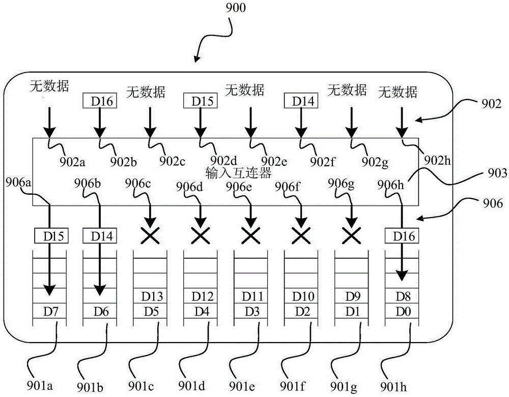
[0068] figure 1 A block diagram of an input interconnector 903 of a storage aggregation device 900 provided in an implementation form is shown.
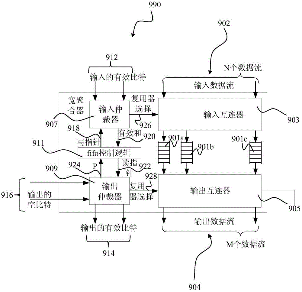
[0069] The memory aggregation device 900, also referred to as a "wide aggregator", is built by a set of N standard FIFOs 901a, 901b, 901c, 901d, 901e, 901f, 901g, and 901h, where these FIFOs are interconnected by two networks Coupled with the input device and the output device respectively. In one implementation form, the interconnected network consists of a set of multiplexers (muxes) at the entry of each FIFO to each output device. The input interconnector 903, also referred to as an ingress interconnector, connects any one of the input devices 902a, 902b, 902c, 902d, 902e, 902f, 902g, and 902h with the FIFO memories 901a, 901b, 901c, 901d , 901e, 901f, 901g and 901h are connected to any data input device, and at the same time, through the fifo control logic unit, the control signal sent to the address of each FIFO is controlled....
PUM
 Abstract
Description
Claims
Application Information
 - R&D Engineer
- R&D Manager
- IP Professional
- Industry Leading Data Capabilities
- Powerful AI technology
- Patent DNA Extraction
Browse by: Latest US Patents, China's latest patents, Technical Efficacy Thesaurus, Application Domain, Technology Topic, Popular Technical Reports.
© 2024 PatSnap. All rights reserved.Legal|Privacy policy|Modern Slavery Act Transparency Statement|Sitemap|About US| Contact US: help@patsnap.com


