Method for producing plated material, and plated material
A manufacturing method and tin plating technology, applied in contact parts, thin material handling, transportation and packaging, etc., can solve the problems of insufficient adhesion between tin plating and silver plating, and achieve excellent wear resistance and electrical conductivity. Effects of low fit, low sliding properties, and excellent wear resistance
- Summary
- Abstract
- Description
- Claims
- Application Information
AI Technical Summary
Problems solved by technology
Method used
Image
Examples
Embodiment 1
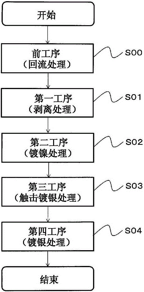
[0141] A 1 μm silver-plated layer was formed on a commercially available reflow tin-plated material (a copper alloy material having a thickness of 0.6 mm tin-plated and subjected to a reflow treatment (first step)) by the following steps. The surface of the tin-plated layer was rinsed by immersing the tin-plated material in a 50° C. cleaning solution containing 40 g / L of MAXCLEENNG-30 manufactured by KIZAI CO., LTD. for 60 seconds.
[0142] Next, the tin-plated material after the above-mentioned cleaning treatment was immersed in a stripping solution at 25°C containing 300 ml / L and 100 ml / L of Ebastrip ST-40A manufactured by JCU Corporation and ST-401NC, respectively, for 60 seconds, and the stripping treatment ( first process). In addition, a masking tape (insulation tape) was attached to the area where peeling was not required to perform masking.
[0143] Next, using a nickel plating bath containing 300 g / L of nickel sulfamate, 5 g / L of nickel chloride hexahydrate, 10 g / L o...
Embodiment 2
[0152] Except having set the time of the nickel plating process to 20 seconds, and having formed the nickel plating layer of thickness 0.1 micrometer, it carried out similarly to Example 1, the plating material was produced, and various evaluations were performed. Table 1 shows the obtained results.
Embodiment 3
[0154] Except having set the time of the silver plating process to 130 seconds, and having formed the plated layer with thickness 5 micrometers, it carried out similarly to Example 2, produced the plated material, and performed various evaluation. Table 1 shows the obtained results.
PUM
| Property | Measurement | Unit |
|---|---|---|
| thickness | aaaaa | aaaaa |
| thickness | aaaaa | aaaaa |
| Vickers hardness | aaaaa | aaaaa |
Abstract
Description
Claims
Application Information
 - R&D
- Intellectual Property
- Life Sciences
- Materials
- Tech Scout
- Unparalleled Data Quality
- Higher Quality Content
- 60% Fewer Hallucinations
Browse by: Latest US Patents, China's latest patents, Technical Efficacy Thesaurus, Application Domain, Technology Topic, Popular Technical Reports.
© 2025 PatSnap. All rights reserved.Legal|Privacy policy|Modern Slavery Act Transparency Statement|Sitemap|About US| Contact US: help@patsnap.com


