Formation method of MOS transistor

A MOS transistor and furnace tube technology, applied in the field of MOS transistor formation, can solve the problems of gate dielectric layer breakdown, gate dielectric layer thickness reduction, semiconductor device performance instability, etc., and achieve growth rate and reliability improvement Effect

Inactive Publication Date: 2016-02-17
SEMICON MFG INT (SHANGHAI) CORP
View PDF5 Cites 0 Cited by
  • Summary
  • Abstract
  • Description
  • Claims
  • Application Information

AI Technical Summary

Problems solved by technology

And once said problem occurs, it will cause unstable performance of the semiconductor device, such as causing time-dependent breakdown (TimeDependentDielectricBreakdown, TDDB) of the gate dielectric layer, especially for non-volatile semiconductor devices, if said problem oc

Method used


Image

  • Formation method of MOS transistor
  • Formation method of MOS transistor
  • Formation method of MOS transistor

Examples


Embodiment Construction

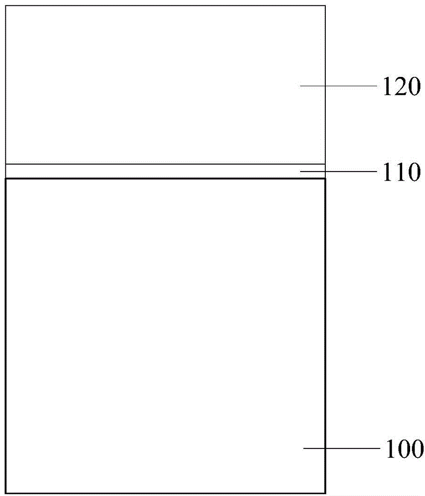
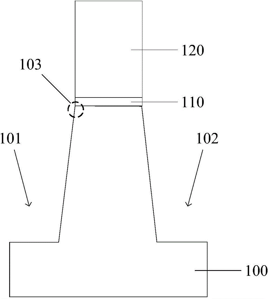
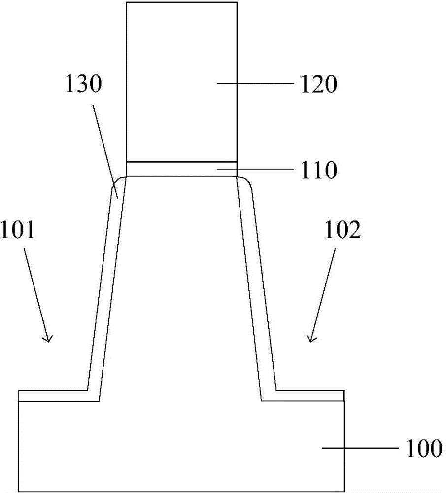
[0032] As mentioned in the background art, when the existing MOS transistor formation method forms a gate dielectric layer on the active region between adjacent shallow trenches, the thickness of the gate dielectric layer at the upper corner of the shallow trenches is generally small, resulting in a MOS transistor Time Dependent Dielectric Breakdown (TDDB) of the gate dielectric layer seriously affects the reliability of semiconductor devices, especially the reliability of non-volatile semiconductor devices.

[0033] The thickness of the gate dielectric layer at the corner on the shallow trench is relatively small, because the growth rate of the gate dielectric layer on the upper surface of the protrusion is relatively fast, while the growth rate on the corner of the shallow trench is relatively slow. The reason is that the upper surface of the active region usually has a crystal orientation, and the density of silicon atoms in this crystal orientation is relatively high, so t...


PUM


Abstract

The invention discloses a formation method of a MOS transistor. The method comprises the following steps: providing a silicon substrate; forming multiple split shallow trenches in the silicon substrate, the region between adjacent shallow trenches being an active region; after the shallow trenches are formed, carrying out silicon ion implantation on the silicon substrate until a silicon-enriched layer at least disposed at the corners of the shallow trenches is formed; after the silicon ion implantation, filling the shallow trenches by use of an insulation material to form a shallow trench isolation structure; forming a gate medium layer on the silicon substrate of the active region; and forming a grid electrode on the gate medium layer. By using the formation method of the MOS transistor, the reliability of the formed MOS transistor can be improved.

Description

technical field [0001] The invention relates to the field of semiconductor manufacturing, in particular to a method for forming a MOS transistor. Background technique [0002] In the manufacture of integrated circuits, the isolation structure is an important technology, and the components formed on the semiconductor substrate must be isolated from other components. With the advancement of semiconductor manufacturing technology, shallow trench isolation (Shallow Trench Isolation, STI) technology has gradually replaced traditional semiconductor device isolation methods such as local oxidation of silicon (LOCOS). [0003] The formation method of the existing shallow trench isolation structure generally includes: oxidizing the wafer (the wafer is the semiconductor substrate) in a high-temperature oxidation furnace tube, forming a pad oxide layer (PadOxide) and a hard mask layer on the semiconductor substrate, and then etching A plurality of discrete shallow trenches are formed ...

Claims


Application Information

Patent Timeline
IPC IPC(8): H01L21/336
Inventor 曹恒金龙灿杨海玩仇圣棻
Owner SEMICON MFG INT (SHANGHAI) CORP
Why Eureka
Try Eureka