Scheduling control method for wafer loading device of semiconductor heat treatment equipment, and system

A technology of heat treatment equipment and scheduling control, applied in manufacturing computing systems, data processing applications, instruments, etc., can solve problems such as the number of uses and cumulative film thickness limitations, and cannot be used multiple times, to ensure machine safety and process quality. Effect

Inactive Publication Date: 2015-12-30
BEIJING NAURA MICROELECTRONICS EQUIP CO LTD
View PDF6 Cites 7 Cited by
  • Summary
  • Abstract
  • Description
  • Claims
  • Application Information

AI Technical Summary

Problems solved by technology

Dummy and ExtraDummy have restrictions on the number of uses and cumulative film thickness, while Product and Monitor can only be used once and cannot be used multiple times

Method used


Image

  • Scheduling control method for wafer loading device of semiconductor heat treatment equipment, and system
  • Scheduling control method for wafer loading device of semiconductor heat treatment equipment, and system
  • Scheduling control method for wafer loading device of semiconductor heat treatment equipment, and system

Examples


Embodiment Construction

[0046] Attached below Figure 1-5 , the specific embodiment of the present invention will be further described in detail.

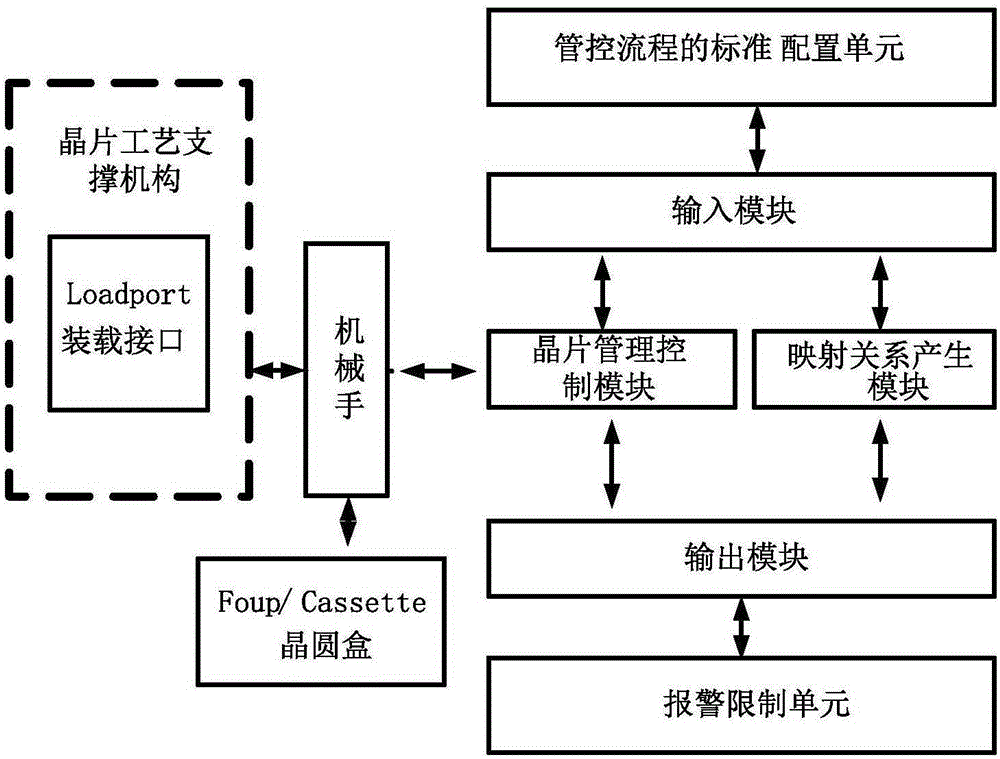
[0047] It should be noted that due to the structural characteristics of semiconductor heat treatment equipment, combined with actual process requirements, it needs to use multiple types of Wafer (Monitor, Product, Dummy, ExtraDummy, etc.) to perform the process at the same time. In the following embodiments, Wafer represents a wafer, Foup and Cassette represent a wafer cassette, LoadPort represents an interface of a wafer process support mechanism on a semiconductor device, and Slot represents a placement position of a wafer in the wafer cassette.

[0048] The scheduling control system of the wafer loading device of the semiconductor heat treatment equipment of the present invention can be realized by hardware or software, preferably, it can be realized by combining software and hardware. In order to be compatible with other control frameworks of semicon...


PUM


Abstract

The invention relates to a scheduling control method for a wafer loading device of semiconductor heat treatment equipment, and a system. The method comprises steps that, a management configuration file of a management and control flow is pre-set or set in real time; a take and put mapping relation between a wafer box and wafers is established according to configuration items in the configuration file, distribution situations of all wafers in the wafer box before loading operation are respectively recorded in a file according to a wafer quantity check mode before displacement; during wafer take and put operation, the wafer management and control flow is established according to the take and put mapping relation and the recorded file, loading and unloading of the wafers relative to the wafer box are carried out through a manipulator, the recorded file is updated in real time according to wafer distribution situations after loading and unloading operation, finally, the recorded file after update is contrasted to determine whether parameters reach or surpass corresponding parameters in the configuration file. According to the method, through software and hardware combination design for the semiconductor equipment, the wafer scheduling management function of the semiconductor diffusion equipment in a non-configured wafer loading device storage bin is realized.

Description

technical field [0001] The present invention relates to the technical field of factory automation (Factory Automation) for semiconductor equipment, more specifically, relates to the technical field of scheduling control management of software systems in semiconductor equipment, in particular a scheduling control method and system for a wafer loading device of semiconductor heat treatment equipment. Background technique [0002] Semiconductor diffusion equipment is an important process equipment for integrated circuit manufacturing. It is an automatic control equipment that requires long-term continuous work, excellent temperature control accuracy, good reliability, and stability. It is suitable for various types of integrated circuit manufacturing. Oxidation, annealing and thin film growth processes. [0003] The factory automation monitoring and management function (FactoryAutomation) of semiconductor equipment is a very important function of semiconductor equipment, and it...

Claims


Application Information

Patent Timeline
Patent Type & Authority Applications(China)
IPC IPC(8): G06Q10/06G06Q50/04
CPCY02P90/30
Inventor 徐冬黄扬君
Owner BEIJING NAURA MICROELECTRONICS EQUIP CO LTD
Why Eureka
Try Eureka