A digital-to-analog converter

A digital-to-analog converter and inverter technology, which is applied in the field of signal processing, can solve the problems of DAC output glitches, the influence of DAC circuit output characteristics, and the unsatisfactory glitch elimination, so as to reduce glitches and improve output characteristics.

Active Publication Date: 2018-05-25
INSPUR BEIJING ELECTRONICS INFORMATION IND
View PDF5 Cites 0 Cited by
  • Summary
  • Abstract
  • Description
  • Claims
  • Application Information

AI Technical Summary

Problems solved by technology

[0003] DAC usually consists of a reference voltage setting device, an analog switch tube, a bit weight network, and an operational amplifier. Among them, the analog switch tube includes a MOS tube, and the MOS tube has a parasitic capacitance. When the dynamic change of the analog switch tube is caused by the conversion of the input signal When , the analog switching tube will release the charge, that is, the charge feedthrough effect, which will cause the DAC to produce glitches in the output, such as figure 1 As shown, the output characteristics of the DAC circuit using this analog switch tube are greatly affected
[0004] In the prior art, in order to reduce the burrs in the DAC output signal, capacitors or filter circuits are usually added to the DAC output to eliminate the burrs. The advantage of this method is that the structure is simple and there is no additional design cost, but the disadvantage is that the burrs are not eliminated enough ideal

Method used


Image

  • A digital-to-analog converter
  • A digital-to-analog converter
  • A digital-to-analog converter

Examples


Embodiment 1

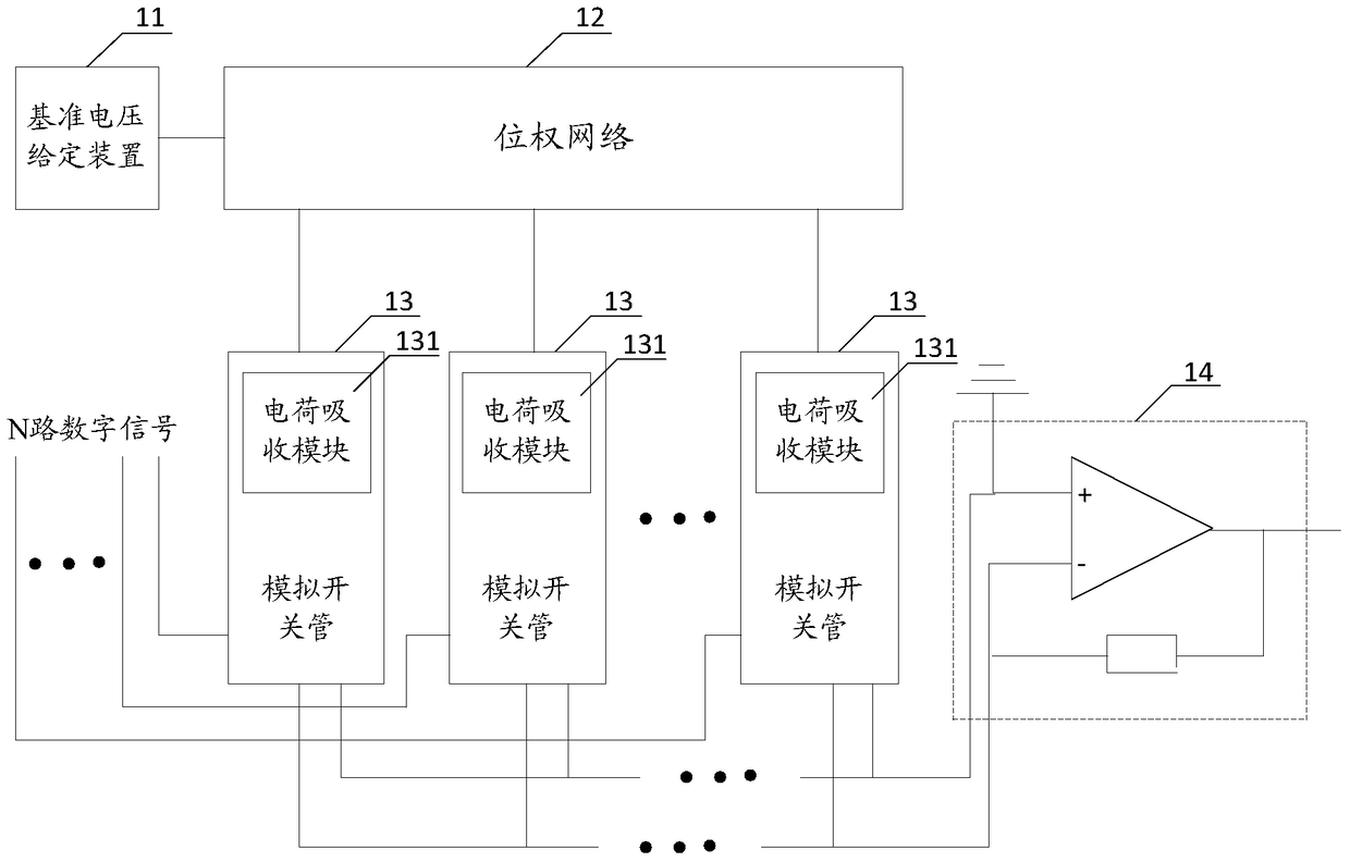
[0038] Please refer to figure 2 , figure 2 A schematic structural diagram of a digital-to-analog converter provided by the present invention;

[0039] The digital-to-analog converter, including:

[0040] The reference voltage setting device 11 is used to provide the reference voltage for the bit weight network 12;

[0041] The bit weight network 12 is connected to the operational amplifier 14 through N analog switch tubes 13, and is used to generate weight currents respectively on the N branches of the bit weight network 12 according to the reference voltage, wherein N is a positive integer;

[0042]N analog switch tubes 13 are used to respectively control the conduction or shutdown between the N branches and the operational amplifier 14 according to N digital signals, wherein each analog switch tube 13 includes an analog switch tube 13 for absorbing A charge absorption module 131 for parasitic charges released during switching transitions;

[0043] It can be understood ...

Embodiment 2

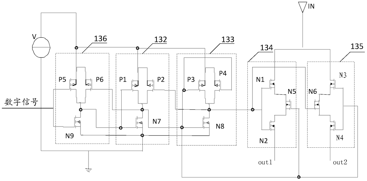
[0049] Please refer to image 3 , image 3 A schematic circuit diagram of an analog switching tube provided by the present invention;

[0050] The digital-to-analog converter provided in this embodiment is based on the previous embodiment:

[0051] Preferably, the charge absorbing module 131 includes a first charge absorbing unit N5 and a second charge absorbing unit N6;

[0052] The analog switch tubes 13 also include a first inverter 132, a second inverter 133, a first switch circuit 134, and a second switch circuit 135, wherein the first charge absorbing unit N5 is located in the first switch circuit 134, and the second The second charge absorption unit N6 is located in the second switch circuit 135;

[0053] The input terminal of the first inverter 132 inputs a digital signal, and the output terminal of the first inverter 132 is connected to the input terminal of the second inverter 133;

[0054] The first switch circuit 134 also includes a first NMOS transistor N1 and...


PUM


Abstract

The invention discloses a digital-to-analog converter, which includes a reference voltage setting device for providing a reference voltage for a bit weight network; and a bit weight network for generating weighted currents on N branches of the bit weight network according to the reference voltage ; N analog switch tubes are used to respectively control the conduction or shutdown between the N branches and the operational amplifier according to the N digital signals. The charge absorption module of the parasitic charge; the operational amplifier is used to sum and amplify the weighted currents of the N branches connected to the operational amplifier, and then convert them into analog current or analog voltage. The charge absorption module will absorb the charge generated by the analog switch tube, providing a discharge channel for the parasitic charge, so as not to affect the output of the digital-to-analog converter, effectively reducing the glitch phenomenon at the output of the digital-to-analog converter, and improving The output characteristics of the digital-to-analog converter.

Description

technical field [0001] The invention relates to the technical field of signal processing, in particular to a digital-to-analog converter. Background technique [0002] DAC (Digital to Analog Converter, digital-to-analog converter), as a device for converting digital signals into analog signals, plays a pivotal role in the field of signal transmission and processing. [0003] DAC usually consists of a reference voltage setting device, an analog switch tube, a bit weight network, and an operational amplifier. Among them, the analog switch tube includes a MOS tube, and the MOS tube has a parasitic capacitance. When the dynamic change of the analog switch tube is caused by the conversion of the input signal When , the analog switching tube will release the charge, that is, the charge feedthrough effect, which will cause the DAC to produce glitches in the output, such as figure 1 As shown, the output characteristics of the DAC circuit using this analog switch tube are greatly af...

Claims


Application Information

Patent Timeline
Patent Type & Authority Patents(China)
IPC IPC(8): H03M1/06H03M1/66
Inventor 王硕
Owner INSPUR BEIJING ELECTRONICS INFORMATION IND
Why Eureka
Try Eureka