Method of reducing white pixels of CMOS image sensor by C ion implantation

An image sensor, ion implantation technology, applied in the direction of electric solid device, semiconductor device, semiconductor/solid state device manufacturing, etc., to reduce white pixels and promote the effect of aggregation

Active Publication Date: 2015-12-23
SHANGHAI HUALI MICROELECTRONICS CORP
View PDF5 Cites 6 Cited by
  • Summary
  • Abstract
  • Description
  • Claims
  • Application Information

AI Technical Summary

Problems solved by technology

[0006] The purpose of the present invention is to overcome the above-mentioned defects in the prior art, and provide a method for reducing the white pixels

Method used


Image

  • Method of reducing white pixels of CMOS image sensor by C ion implantation
  • Method of reducing white pixels of CMOS image sensor by C ion implantation
  • Method of reducing white pixels of CMOS image sensor by C ion implantation

Examples


Embodiment Construction

[0027] The specific embodiment of the present invention will be further described in detail below in conjunction with the accompanying drawings.

[0028] It should be noted that, in the following specific embodiments, when describing the embodiments of the present invention in detail, in order to clearly show the structure of the present invention for the convenience of description, the structures in the drawings are not drawn according to the general scale, and are drawn Partial magnification, deformation and simplification are included, therefore, it should be avoided to be interpreted as a limitation of the present invention.

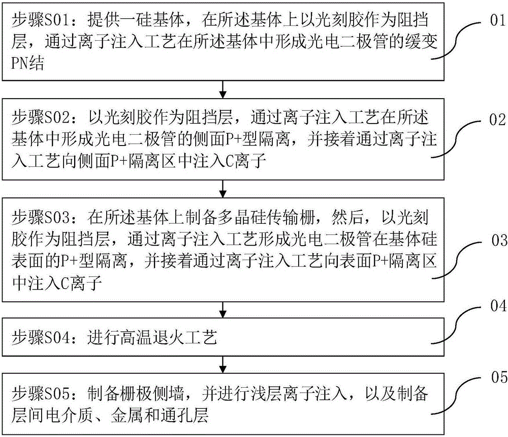
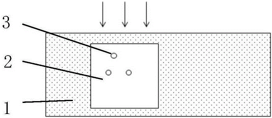
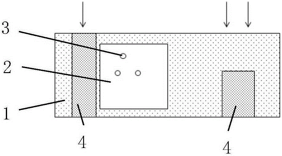
[0029] In the following specific embodiments of the present invention, please refer to figure 1 , figure 1 It is a flow chart of the method for reducing white pixels of a CMOS image sensor by C ion implantation in the present invention; at the same time, please refer to Figure 2 to Figure 9 , Figure 2 to Figure 9 is a preferred embodiment of the...


PUM


Abstract

The present invention discloses a method of reducing the white pixels of a CMOS image sensor by C ion implantation. In allusion to the problem that the white pixels of the conventional CMOS image sensor are more, and by an ion implantation technology, the C ions of a certain concentration are implanted in a P+ type isolation region around a photodiode, and by a high temperature annealing process, the aggregation of the C ions to the oxygen in the P+ type isolation region and the adsorption of the oxygen precipitation formed by the oxygen aggregation to the metal ion pollution in the photodiode are promoted, thereby being able to reduce the white pixels of the CMOS image sensor effectively.

Description

technical field [0001] The invention relates to the technical field of semiconductor integrated circuit manufacturing, and more particularly, relates to a process integration method for reducing white pixels of a CMOS image sensor through C ion implantation. Background technique [0002] With the rapid development of the mobile Internet, people's demand for smart terminals is increasing, and image sensors, known as the "eyes" of smart terminals, have also ushered in unprecedented development space. Due to its high power consumption, traditional CCD image sensors are limited in the market for high-performance digital cameras; CMOS image sensors not only have low power consumption and fast speed, but also are easy to be compatible with existing semiconductor processes and have low production costs. This makes CMOS image sensors occupy half of the image sensor market. [0003] The future direction of CMOS image sensor development is high pixel, low power consumption, high imag...

Claims


Application Information

Patent Timeline
IPC IPC(8): H01L21/266H01L21/8238H01L27/146
CPCH01L21/266H01L21/8238H01L21/823878H01L27/14645H01L27/14687
Inventor 范晓陈昊瑜田志
Owner SHANGHAI HUALI MICROELECTRONICS CORP
Why Eureka
Try Eureka